Semiconductor device

Inactive Publication Date: 2010-03-11
RENESAS ELECTRONICS CORP
View PDF0 Cites 12 Cited by
  • Summary
  • Abstract
  • Description
  • Claims
  • Application Information

AI Technical Summary

Benefits of technology

[0010]In the semiconductor device according to the aspect of the present invention, the compensation capacitance elements are formed over an upper layer of the second region excluding upper layer portions of the drain diffusion layers or the gate electrodes of the transistors. This makes it possib

Problems solved by technology

Due to an increase in circuit scale and operation speed of semiconductor devices in recent years, consumption current is increasing.
In such semiconductor devices, however, since even a slight variation in supply voltage has a great impact on the supply voltage, a problem comes to the surface that the variation in supply voltage causes an unstable circuit operation.
However, if the compensation capacitance elements are disposed in the vicinity of signal paths in the case where the compensation capacitance

Method used


Image

  • Semiconductor device
  • Semiconductor device
  • Semiconductor device

Examples


first embodiment

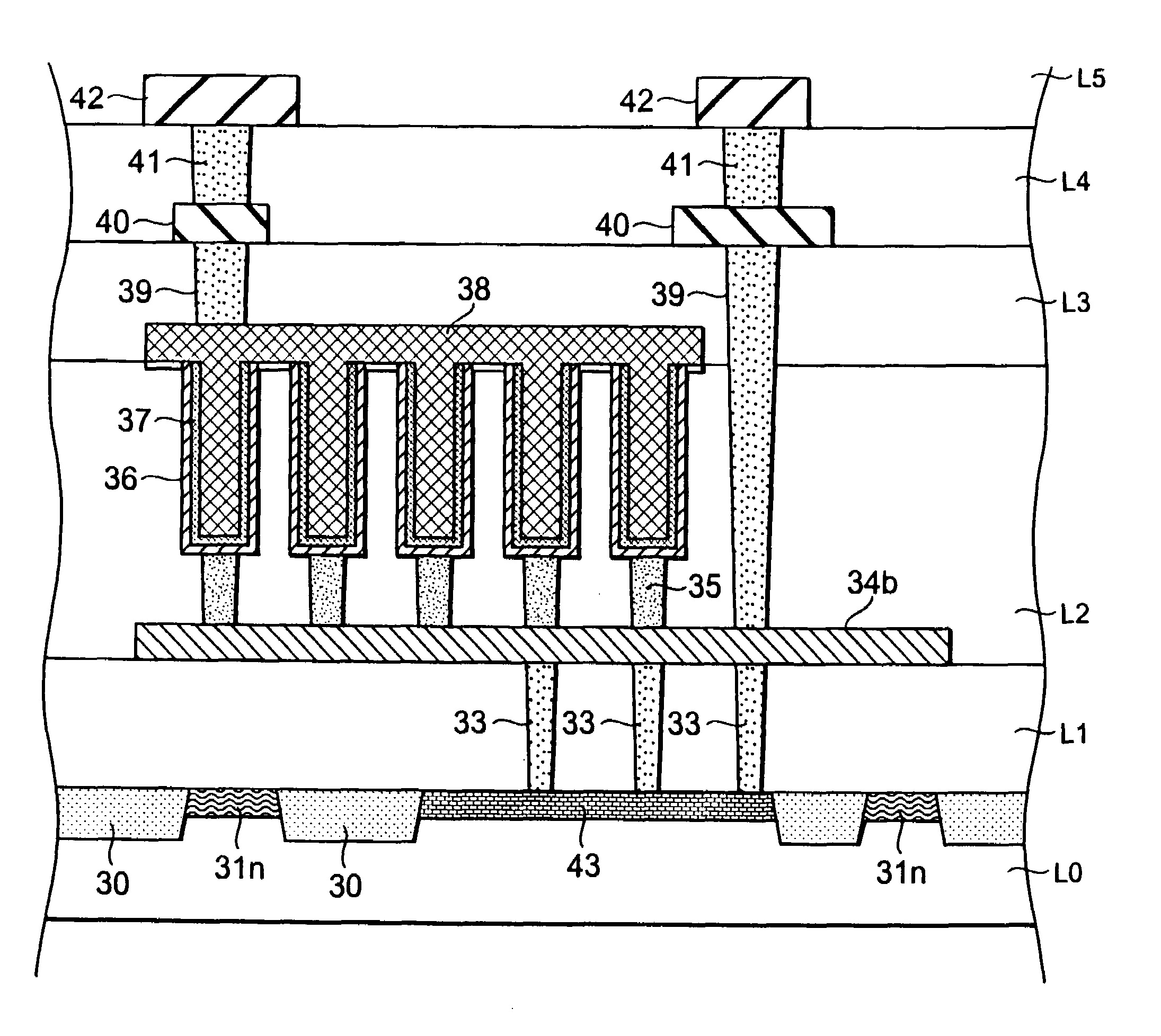
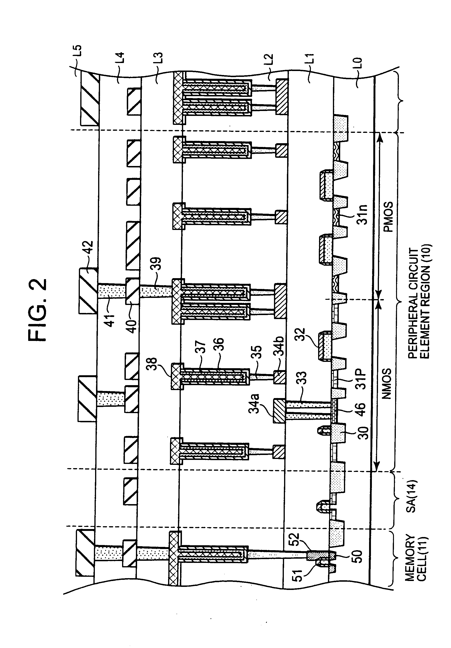
[0018]Hereinafter, a first embodiment of the present invention will be described with reference to the accompanying drawings. FIG. 1 shows a schematic view of a semiconductor device 1 according to the first embodiment. As shown in FIG. 1, the semiconductor device 1 includes second regions (e.g. peripheral circuit element regions) 10, third regions (e.g. regions other than the peripheral circuit element regions) 20, and a first region (e.g. memory cell region).

[0019]In each of the peripheral circuit element regions 10, a functional circuit for realizing the function of the semiconductor device 1 is disposed. The functional circuit includes transistors, resistors, and capacitors. The capacitors include compensation capacitance elements for suppressing a variation in supply voltage. In each of the regions 20 other than the peripheral circuit element regions, no semiconductor elements forming a functional circuit are disposed, that is, the regions 20 are so-called free spaces. In this e...

second embodiment

[0037]FIG. 6 illustrates an example of the plan layout of compensation capacitance elements on a semiconductor device according to a second embodiment of the present invention. FIG. 6 is the modified plan layout of the plan layout of FIG. 4, in accordance with the second embodiment. Although the compensation capacitance elements according to the first embodiment are disposed in the regions on the peripheral circuit element region 10 excluding the upper layer portions of the transistors, the compensation capacitance elements according to the second embodiment are also disposed above the source diffusion layers of the transistors, as well as in the former regions.

[0038]In the plan layout according to the second embodiment, as shown in FIG. 6, the compensation capacitance elements are also disposed above a part of the source diffusion layers of the transistors provided in the peripheral circuit element region 10. By expanding the layout regions of the compensation capacitance elements ...


PUM


Abstract

A semiconductor device is proposed in which signal delay due to compensation capacitance elements in peripheral circuit element regions is eliminated. The semiconductor device includes: a first region including memory cells; a second region 10 including a functional circuit; cell capacitors formed in the first region; and compensation capacitance elements 36 to 38 formed in the second region 10, wherein the compensation capacitance elements 36 to 38 each include a lower electrode 36, a capacitance insulating film 37, and an upper electrode 38, the lower electrode 36, capacitance insulating film 37, and upper electrode 38 being the same as those of the cell capacitors, and wherein the compensation capacitance elements are formed over an upper layer of the second region 10 excluding upper layer portions of drain diffusion layers 44, 46 or gate electrodes 32 of transistors in the functional circuit.

Description

BACKGROUND OF THE INVENTION[0001]1. Field of the Invention[0002]The present invention relates to a semiconductor device, and more particularly, to a semiconductor device incorporating compensation capacitance elements connected between two wirings for compensating a potential variation in wirings.[0003]2. Description of the Related Art[0004]Due to an increase in circuit scale and operation speed of semiconductor devices in recent years, consumption current is increasing. Thus, a variation in supply voltage has been increased. On the other hand, there has been an increasing trend to lower the operating supply voltage for semiconductor devices. In such semiconductor devices, however, since even a slight variation in supply voltage has a great impact on the supply voltage, a problem comes to the surface that the variation in supply voltage causes an unstable circuit operation.[0005]Therefore, it has been proposed that compensation capacitance elements provided between a power supply wi...

Claims


Application Information

Patent Timeline
IPC IPC(8): H01L27/108
CPCH01L23/5223H01L24/05H01L28/40H01L27/10894H10B12/09
Inventor MIZUSHIMA, HIROAKI
Owner RENESAS ELECTRONICS CORP
Why Eureka
Try Eureka