Test structure for detection of defect devices with lowered resistance

Active Publication Date: 2010-03-11
NXP BV
View PDF20 Cites 12 Cited by
  • Summary
  • Abstract
  • Description
  • Claims
  • Application Information

AI Technical Summary

Benefits of technology

[0031]An advantage of the test structure of the present embodiment in comparison with a test structure for identifying opens as disclosed in U.S. Pat. No. 6,392,251 is that it is simpler to identify the defect DUTs from the total electrical resistance of the test structure for any combination of defect DUTs in the test structure. For the test structure of the present embodiment enables determining the number of defect DUTs by measuring a current flow through the test structure between the test contact pads at a given voltage between the test contact pads. Each DUT in the defect state raises the current flow by a step determined by the electrical test resistance of the test resistor. In contrast, identifying an open of a via as in U.S. Pat. No. 6,392,251 requires a repetitive calculation of different test resistor combinations and a subsequent comparison wit

Problems solved by technology

This mechanical movement is very time-consuming, and due to the large number of test contact pads a correspondingly large area of the substrate is consumed.
Additionally, the testing

Method used


Image

  • Test structure for detection of defect devices with lowered resistance
  • Test structure for detection of defect devices with lowered resistance
  • Test structure for detection of defect devices with lowered resistance

Examples


Embodiment Construction

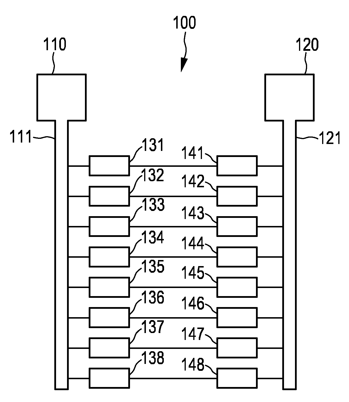
[0074]FIG. 1 shows a schematic view of an embodiment of a test structure 100. The test structure 100 comprises a first test contact pad 110, which is connected with a first conducting line 111. Furthermore, the test structure 100 comprises a second test contact pad 120, which is connected with a second conducting line 121. The first and second conducting lines 111 and 121 are parallel to each other and rectilinear, and preferably arranged on an identical metal level. DUTs 131 to 138 branch off in parallel from the first and second conducting lines 111 and 121.

[0075]The DUTs are shown as blocks in the schematic representation of the test structure of FIG. 1. The DUTs may take the form of, for example, comb-comb structures, diodes, transistors, varistors, capacitors etc. The DUTs are drawn as 2-terminal devices in FIG. 1. However, the can contain dependent or independent additional terminals. More specific examples of DUTs will be given below in FIG. 2 and FIG. 3 and the pertaining de...


PUM


Abstract

The present invention relates to a test structure that comprises at least two devices under test DUT, which respectively have a first electrical device resistance in a non-defect state and a second electrical device resistance in defect state, the first being higher than the second electrical device resistance. In the test structure the DUTs are connected in parallel to a first test contact pad via a first conducting line and connected in parallel to a second test contact pad via a second conducting line, and respectively connected to the first conducting line via respective first test resistors, which have known respective electrical test resistances, such that a total electrical resistance between the first an second test contact pads is indicative of the number of DUTs, which have the second electrical device resistance. The test structure allows testing a larger number of DUTs in parallel in a single measurement.

Description

FIELD OF THE INVENTION[0001]The invention relates to a test structure comprising at least two devices under test, hereinafter DUTs, which respectively have a first electrical device resistance in a non-defect state and a second electrical device resistance in defect state. The invention further relates to a substrate comprising at least one integrated circuit and one or more test structures a test method.BACKGROUND OF THE INVENTION[0002]In the production process of integrated circuits devices are tested to estimate the device yields and possible yield-detracting processing problems. Since the production of integrated circuits comprises many processing steps and different technologies, the technological sources of electrical failure such as short circuits within the integrated circuits or open contacts are investigated using test structures in order to estimate a suitable process window and to improve the device quality as well as the processing yield.[0003]It is therefore desirable ...

Claims


Application Information

Patent Timeline
IPC IPC(8): G01R31/02G01R27/08
CPCG01R31/2831H01L2924/3011H01L22/34G01R31/2884
Inventor DE VRIES, DIRK KENNETHGONELLA, ROBERTO MAURIZIO
Owner NXP BV
Why Eureka
Try Eureka