Switch-less bidirectional amplifier

a bidirectional amplifier and switchless technology, applied in the direction of two-way amplifiers, gated amplifiers, amplifiers with field-effect devices, etc., can solve the problems of signal loss, signal loss has a negative impact on the linearity and noise figure of the transceiver circuit, and switches occupy valuable area on the circuit chip. achieve the effect of reducing chip area and high electron mobility

Active Publication Date: 2010-03-11
TELEFON AB LM ERICSSON (PUBL)
View PDF2 Cites 7 Cited by
  • Summary
  • Abstract
  • Description
  • Claims
  • Application Information

AI Technical Summary

Benefits of technology

[0011]In this fashion use of switches which normally entails signal losses in an amplification circuit and leakage currents is avoided.
[0014]Apart from that, these at least two biased semiconductor amplification elements may be connected so as to provide parallel feedback. Parallel feedback is a simple way of achieving equal input and output impedance in the circuit in order to avoid signal reflections due to impedance mismatch. Impedance matching is important when the bi-direction amplifier is to be used in a microwave-based communication circuit.
[0016]However, these biased semiconductor amplification elements may equally be integrated into an integrated circuit device. Especially in integrated circuits common in microwave applications, so called MMICs (Monolithic Microwave Integrated Circuits), the use of the bi-directional amplifier according to the present invention is advantageous, since MMIC switches which are normally necessary for switching the direction of signal amplification are thereby made obsolete. Also, the integrated solution for the bi-directional amplifier according to the invention would further reduce the area occupied on the chip by the bi-directional amplifier.
[0020]The advantage of this configuration is the possibility to use the bi-directional amplifier to direct and amplify a signal in a desired direction without the disadvantages introduced when using a switch.
[0024]The main advantage of the three configurations mentioned above is the avoidance of the use of switches taking up valuable space on the chip while at the same time being able to both direct and amplify a signal in the desired direction irrespective whether it is a received signal or a signal to be transmitted by the circuit. The last configuration mentioned above would make it possible to direct and amplify signal form any direction into any other direction without using switches.

Problems solved by technology

However, when using active components one encounters a problem, since amplifiers by definition are non-reciprocal.
The problem with such a configuration is that the switches occupy valuable area on the circuit chip and introduce signal losses.
These signal losses have a negative impact on the linearity and the noise figure of the transceiver circuit.
Moreover, the switches exhibit a more or less unpredictable current leakage which degrades the performance of such a transceiver circuit.
This solution however, is not a true bidirectional solution, since the amplifiers in both groups always amplify a signal in one direction only.
Also, the amount of amplifiers takes up valuable space on the circuit board.
However, this solution also is not really a bidirectional solution either, since the amplifiers only amplify the signal in one direction.
The four-port and above all the cross-coupled structure described also introduce undesired signal losses.
However, since the transistor is connected in “common-gate” mode to the rest of the circuit, additional output impedance compensation circuitry is needed to keep the output of the transistor amplifier stable, thus taking up additional valuable space on the circuit board or chip.
Apart from adding one more transistor to the circuit board which occupies additional space and adds to the noise figure of the amplified signal, an additional variable impedance matching network is needed in order to match the output impedance of the one of the transistors to the input impedance of one other transistor adding to the complexity of the circuit.

Method used


Image

  • Switch-less bidirectional amplifier
  • Switch-less bidirectional amplifier
  • Switch-less bidirectional amplifier

Examples


Embodiment Construction

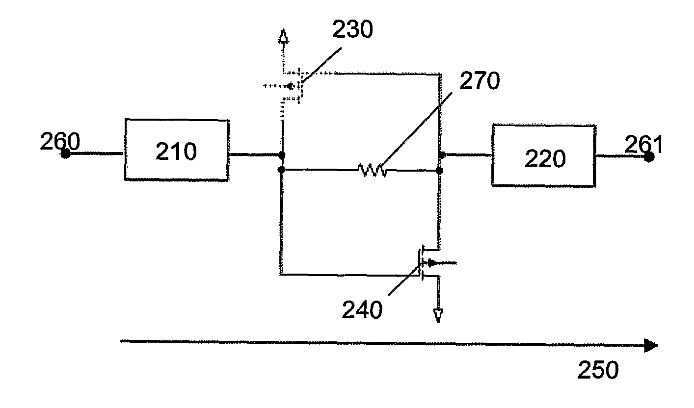
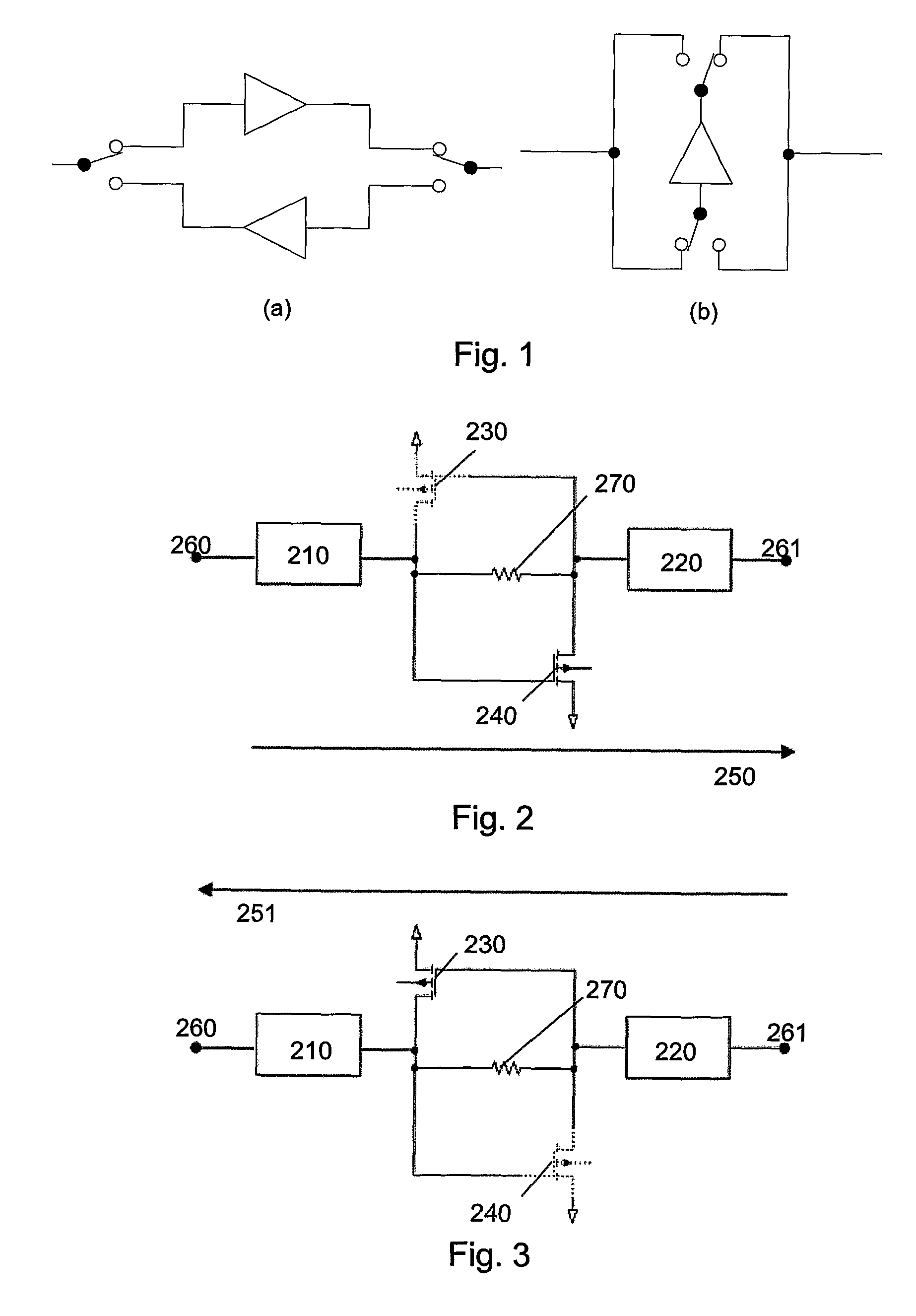
[0052]Turning now to FIG. 2, a first embodiment of the present invention is shown. Here, an example of the inventive bi-directional amplifier is shown, where reference numbers 230 and 240 depict a first and a second transistor connected in an anti-parallel configuration in relation to each other using parallel feedback.

[0053]Anti-parallel in this case means the gate terminal of the first transistor 230 is connected to the drain terminal of the second transistor and the gate terminal of the second transistor 240 is connected to the drain terminal of the first transistor 230. The resistor 270 between the first and second transistors (230, 240) is one way of achieving equal impedance for the two transistors. Of course any other means, such as an impedance matching network may be used to achieve the equal input impedance for the two transistors.

[0054]Even though the embodiments of the present invention described in the accompanying drawings use FETs (Field Effect Transistors) as amplifi...


PUM


Abstract

A bi-directional amplifier, transceiver, integrated circuit, mobile unit, telecommunication infrastructure for amplification of signals received or signals to be transmitted in a communication circuit and a method for bi-directional amplification comprising amplifying signals in a bi-directional amplifier and directing a signal between two or more different paths comprising at least one first biased semiconductor amplification element coupled to a at least one first impedance matching network, at least one second biased semiconductor amplification element coupled to a second impedance matching network, a first device for biasing the at least one first biased semiconductor amplification element and a second device for biasing the at least one second biased semiconductor amplification element where the direction of signal amplification in said bi-directional amplifier is controlled by the first or second device for biasing the at least one first or second biased semiconductor amplification element.

Description

TECHNICAL FIELD[0001]The present invention relates to bidirectional amplifiers as they are for example used in microwave transceivers.BACKGROUND OF THE INVENTION[0002]At present in the field of microwave systems equipped with a common receive and transmit antenna it is desired to use a common leg for both transmit and receive signal paths. This is not a problem when using passive reciprocal components. However, when using active components one encounters a problem, since amplifiers by definition are non-reciprocal. Normally, one uses external switches and one or two amplifiers to switch between signal paths and amplification in one or the other direction.[0003]An illustration of this principle is given in the form of two examples in FIG. 1.[0004]The problem with such a configuration is that the switches occupy valuable area on the circuit chip and introduce signal losses. These signal losses have a negative impact on the linearity and the noise figure of the transceiver circuit. Mor...

Claims


Application Information

Patent Timeline
Patent Type & Authority Applications(United States)
IPC IPC(8): H03F3/04
CPCH03F1/56H03F3/195H03F3/62H03F2203/7206H03F2200/222H03F2200/387H03F2200/451H03F3/72
Inventor BERG, HAKANTHIESIES, HEIKO
Owner TELEFON AB LM ERICSSON (PUBL)
Why Eureka
Try Eureka