Method for tuning a deposition rate during an atomic layer deposition process

a technology of atomic layer and deposition rate, which is applied in the direction of chemical vapor deposition coating, coating, special surfaces, etc., can solve the problems of pvd process reaching a limit at this size and aspect ratio, many challenges to process control, lack of stability of deposition rate and minumium control, etc., and achieve the effect of reducing the deposition rate of the material

Inactive Publication Date: 2010-03-11
APPLIED MATERIALS INC
View PDF99 Cites 49 Cited by
  • Summary
  • Abstract
  • Description
  • Claims
  • Application Information

AI Technical Summary

Benefits of technology

[0010]Embodiments of the invention provide methods for depositing a material on a substrate within a processing chamber during a vapor deposition process, such as an atomic layer deposition (ALD) process. Generally, the substrate may be continuously or periodically exposed to a treatment gas containing a reagent prior to and/or during the vapor deposition process. The deposition rate of the material being ...

Problems solved by technology

Tantalum-containing layers, such as tantalum, tantalum nitride, and tantalum silicon nitride, are often used in multi-level integrated circuits and pose many challenges to process control, particularly with respect to contact formation.
However, it is believed that PVD processes may have reached a limit at this size and aspect ratio, while ALD proc...

Method used


Image

  • Method for tuning a deposition rate during an atomic layer deposition process
  • Method for tuning a deposition rate during an atomic layer deposition process
  • Method for tuning a deposition rate during an atomic layer deposition process

Examples


Embodiment Construction

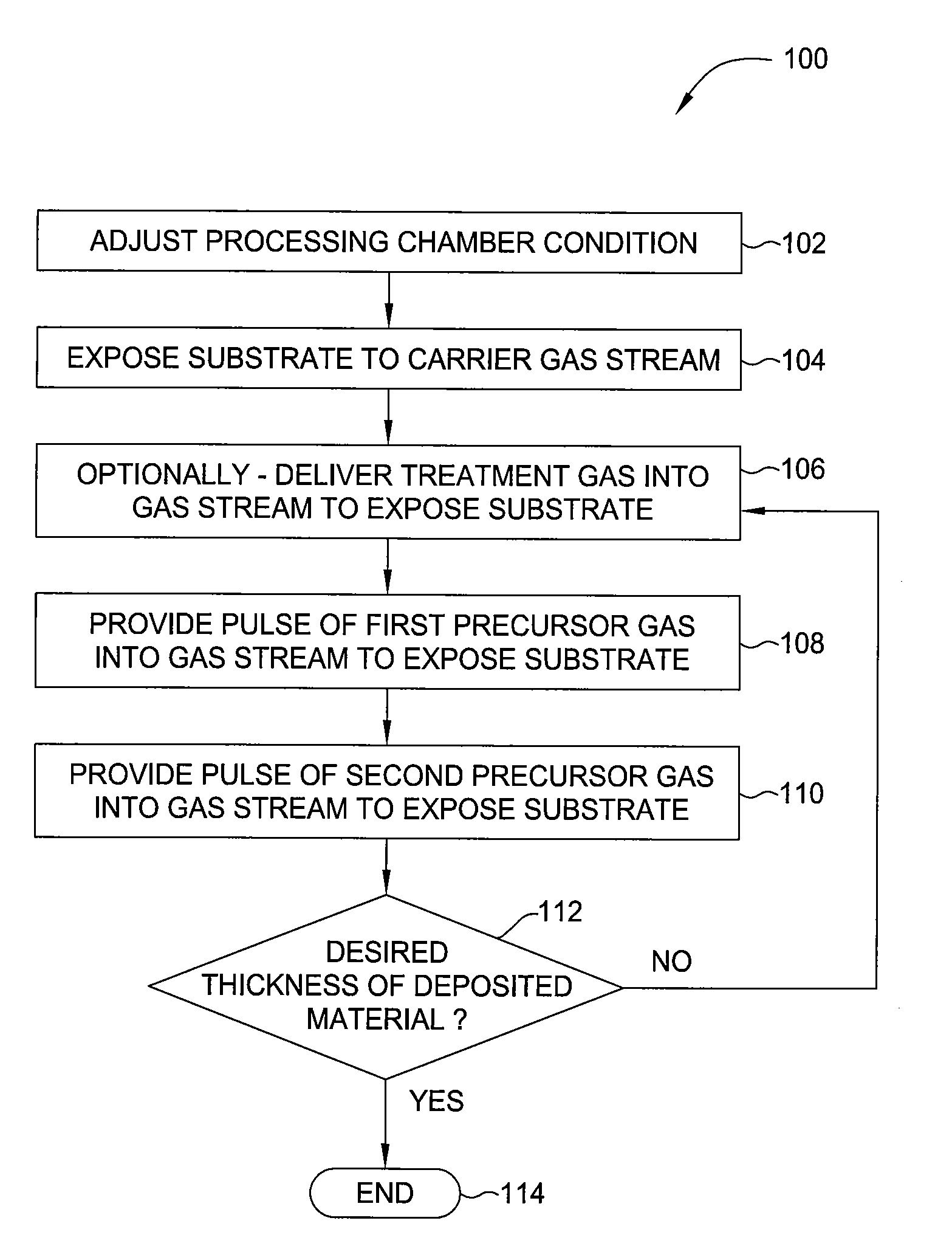
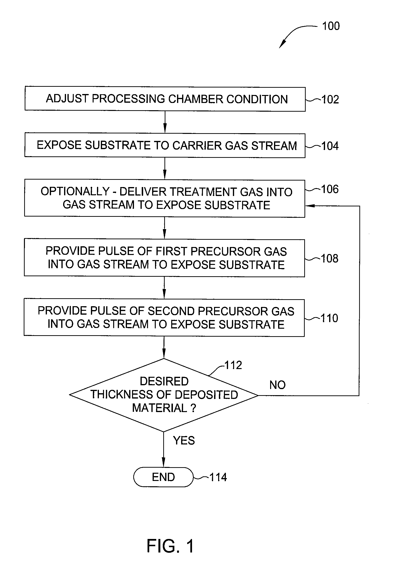
[0025]Embodiments of the invention provide methods for depositing a material on a substrate within a processing chamber during a vapor deposition process, such as an atomic layer deposition (ALD) process or a chemical vapor deposition (CVD) process. Generally, the substrate may be continuously or periodically exposed to a treatment gas containing a reagent prior to and / or during the vapor deposition process. The treatment gas may be administered into the processing chamber and the substrate is exposed to the treatment gas prior to and / or during the vapor deposition process. The deposition rate of the material being deposited may be controlled by varying the amount of treatment gas exposed to the substrate. Therefore, the deposition rate may be adjusted, such as within a range from about 0.05 Å / cycle (Å per ALD cycle) to about 1.0 Å / cycle, for example, about 0.5 Å / cycle.

[0026]In one example, the method includes exposing the substrate to the treatment gas to reduce the depos...


PUM

PropertyMeasurementUnit
Fractionaaaaaaaaaa
Deposition rateaaaaaaaaaa

Abstract

Embodiments of the invention provide methods for depositing a material on a substrate within a processing chamber during a vapor deposition process, such as an atomic layer deposition (ALD) process. In one embodiment, a method is provided which includes sequentially exposing the substrate to a first precursor gas and at least a second precursor gas while depositing a material on the substrate during the ALD process, and continuously or periodically exposing the substrate to a treatment gas prior to and/or during the ALD process. The deposition rate of the material being deposited may be controlled by varying the amount of treatment gas exposed to the substrate. In one example, tantalum nitride is deposited on the substrate and the alkylamino metal precursor gas contains a tantalum precursor, such as pentakis(dimethylamino) tantalum (PDMAT), the second precursor gas contains a nitrogen precursor, such as ammonia, and the treatment gas contains dimethylamine (DMA).

Description

CROSS-REFERENCE TO RELATED APPLICATIONS[0001]This application is a continuation-in-part of U.S. Ser. No. 12 / 206,705 (APPM / 12256), filed Sep. 8, 2008, which is herein incorporated by reference.BACKGROUND OF THE INVENTION[0002]1. Field of the Invention[0003]Embodiments of the invention generally relate to semiconductor and other electronic device processing, and more particularly, to an improved method for depositing a material on a substrate during a vapor deposition process.[0004]2. Description of the Related Art[0005]The electronic device industry and the semiconductor industry continue to strive for larger production yields while increasing the uniformity of layers deposited on substrates having increasingly larger surface areas. These same factors in combination with new materials also provide higher integration of circuits per unit area on the substrate. The need for greater deposition rate and process control regarding layer characteristics rises as the desire for an increased ...

Claims


Application Information

Patent Timeline
IPC IPC(8): B05D5/12
CPCC23C16/45534H01L21/76841C23C16/52
Inventor MA, PAULAUBUCHON, JOSEPH F.LU, JIANGCHANG, MEI
Owner APPLIED MATERIALS INC
Why Eureka
Try Eureka