
Photoelectric conversion device and method for manufacturing the same

a technology of photoelectric conversion device and manufacturing method, which is applied in the field of photoelectric conversion device and a manufacturing method for the same, can solve the problems of non-single-crystal silicon thin films such as thin microcrystalline silicon films, which have defects serving as carrier traps, and the supply of silicon is very short, so as to improve the photoelectric conversion efficiency of a photoelectric conversion device having a non-single-crystal semiconductor layer. the effect of defects

Inactive Publication Date: 2010-04-01
SEMICON ENERGY LAB CO LTD
View PDF15 Cites 11 Cited by
  • Summary
  • Abstract
  • Description
  • Claims
  • Application Information

AI Technical Summary

Benefits of technology

[0010]In view of the above problems, it is an object of one embodiment of the present invention to form a non-single-crystal semiconductor layer in which defects are reduced, as a semiconductor layer forming a semiconductor junction of a photoelectric conversion device. It is another object of an embodiment of the present invention to improve photoelectric conversion efficiency of a photoelectric conversion device formed using a non-single-crystal semiconductor layer.
[0024]According to one embodiment of the present invention, a photoelectric conversion device having, as a photoelectric conversion layer, a non-single-crystal semiconductor layer in which defects are reduced can be provided. Further, photoelectric conversion efficiency of a photoelectric conversion device having a non-single-crystal semiconductor layer can be improved.

Problems solved by technology

Further, in recent years, silicon has been in very short supply for recovery of the semiconductor market and for rapid growth of the solar cell market.
From such aspects, bulk photoelectric conversion devices of crystal silicon have difficulty in resource saving and cost reduction.
However, non-single-crystal silicon thin films such as thin amorphous silicon films and thin microcrystalline silicon films have defects serving as carrier traps, such as dangling bonds and crystal grain boundaries.
Therefore, it is difficult to obtain sufficient photoelectric conversion efficiency, and thus, bulk photoelectric conversion devices of crystal silicon have got a larger share in the solar cell market.

Method used


Image

  • Photoelectric conversion device and method for manufacturing the same
  • Photoelectric conversion device and method for manufacturing the same
  • Photoelectric conversion device and method for manufacturing the same

Examples


embodiment 1

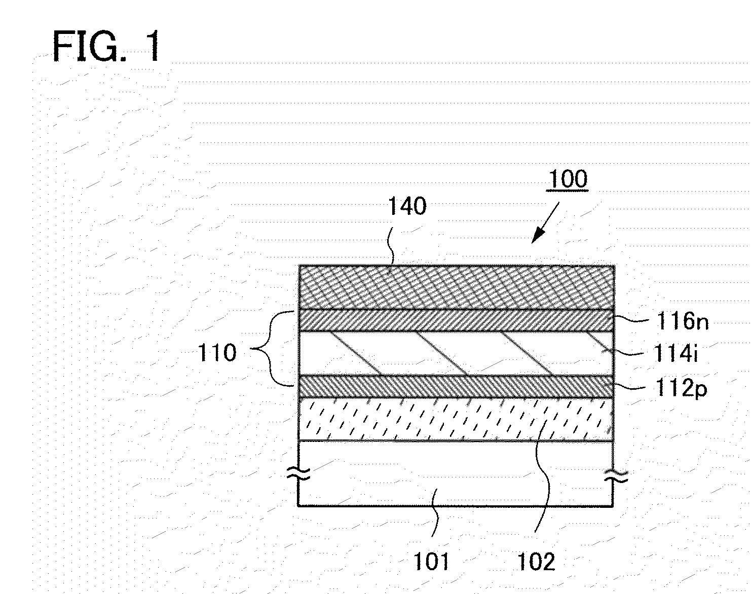
[0041]FIG. 1 illustrates an example of a schematic cross-sectional view of a photoelectric conversion device 100 of this embodiment.

[0042]The photoelectric conversion device 100 illustrated in FIG. 1 has a structure in which a unit cell 110 is interposed between a first electrode 102 and a second electrode 140 which are provided over a substrate 101. In the unit cell 110, a non-single-crystal semiconductor layer 114i is provided between a first impurity semiconductor layer 112p and a second impurity semiconductor layer 116n, and the unit cell 110 includes at least one semiconductor junction. As the semiconductor junction, a p-i-n junction is typically given.

[0043]The non-single-crystal semiconductor layer 114i is a semiconductor layer in which the nitrogen concentration, the oxygen concentration, and the carbon concentration are controlled. In the non-single-crystal semiconductor layer 114i, the nitrogen concentration is within a predetermined range and the oxygen concentration and ...

embodiment 2

[0105]In this embodiment, a photoelectric conversion device having a structure different from the structure described in the above embodiment is described. In specific, an example in which an amorphous semiconductor layer is formed between the first impurity semiconductor layer 112p and the non-single-crystal semiconductor layer 114i is described.

[0106]In the photoelectric conversion device illustrated in FIG. 6, the first electrode 102, the first impurity semiconductor layer 112p, an amorphous semiconductor layer 113, the non-single-crystal semiconductor layer 114i, the second impurity semiconductor layer 116n, and the second electrode 140 are stacked in this order from the first substrate 101 side. In this embodiment, the amorphous semiconductor layer 113 is provided between the first impurity semiconductor layer 112p and the non-single-crystal semiconductor layer 114i.

[0107]By providing the amorphous semiconductor layer 113 between the first impurity semiconductor layer 112p and...

embodiment 3

[0111]In this embodiment, a photoelectric conversion device having a structure different from the structures described in the above embodiments is described. In specific, an example in which the number of unit cells to be stacked is different from that in the photoelectric conversion device illustrated in FIG. 1 is described.

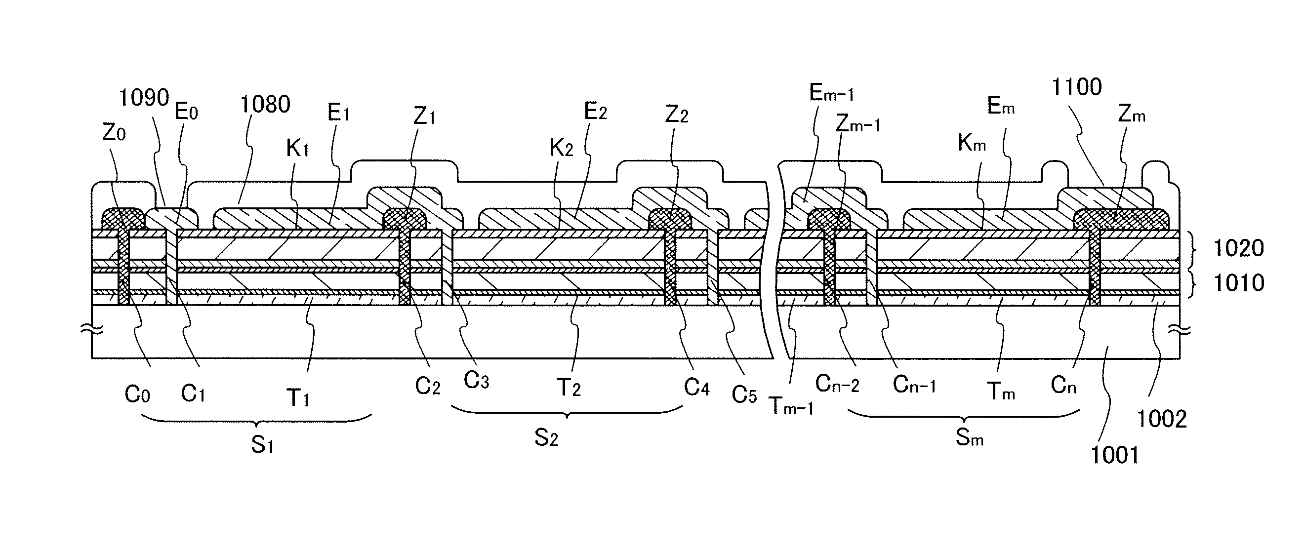
[0112]FIG. 7 is a tandem photoelectric conversion device 200 in which two unit cells are stacked. The photoelectric conversion device 200 includes the unit cell 110 formed over the substrate 101 provided with the first electrode 102, a unit cell 220 formed over the unit cell 110, and a second electrode 140 formed over the unit cell 220.

[0113]The unit cell 110 has a structure in which the first impurity semiconductor layer 112p, the non-single-crystal semiconductor layer 114i, and the second impurity semiconductor layer 116n are stacked in this order from the first electrode 102 side. The non-single-crystal semiconductor layer 114i included in the unit cell 110 i...


PUM


Abstract

A photoelectric conversion device includes one or more unit cells between a first electrode and a second electrode, in which a semiconductor junction is formed by sequentially stacking: a first impurity semiconductor layer of one conductivity type; an intrinsic non-single-crystal semiconductor layer including an NH group or an NH2 group; and a second impurity semiconductor layer of opposite conductivity type to the first impurity semiconductor layer. In the non-single-crystal semiconductor layer of a unit cell on a light incident side, the nitrogen concentration measured by secondary ion mass spectrometry is 5×10¹⁸ / cm3 or more and 5×10²⁰ / cm3 or less and oxygen and carbon concentrations measured by secondary ion mass spectrometry are less than 5×10¹⁸ / cm3.

Description

BACKGROUND OF THE INVENTION[0001]1. Field of the Invention[0002]The present invention relates to a photoelectric conversion device and a method for manufacturing the same.[0003]2. Description of the Related Art[0004]In order to take measures against global environmental issues including global warming, the market for photoelectric conversion devices typified by solar cells has expanded. Bulk photoelectric conversion devices of crystal silicon which achieve high photoelectric conversion efficiency have already been put into practical use. For bulk photoelectric conversion devices of crystal silicon, bulk silicon substrates such as single crystal silicon substrates or polycrystalline silicon substrates are used. However, most part of a bulk silicon substrate serves as a support which does not contribute to photoelectric conversion. Further, in recent years, silicon has been in very short supply for recovery of the semiconductor market and for rapid growth of the solar cell market. Fro...

Claims


Application Information

Patent Timeline
IPC IPC(8): H01L31/0368H01L31/18H01L21/205H01L31/06H01L31/075
CPCH01L31/075H01L31/1824Y02E10/548Y02E10/545H01L31/202Y02P70/50
Inventor MIYAIRI, HIDEKAZUHIROHASHI, TAKUYASHIMOMURA, AKIHISA
Owner SEMICON ENERGY LAB CO LTD
Learn More