Semiconductor component with contacts made of alloyed-in metal wires

a technology of metal wires and components, applied in the field of semiconductor components, can solve problems such as efficiency reduction, and achieve the effects of reducing resistance losses, high electrical conductivity, and reducing cross-sectional surface area of contact structures

Inactive Publication Date: 2010-04-01
SOLARWORLD IND GMBH
View PDF8 Cites 12 Cited by
  • Summary
  • Abstract
  • Description
  • Claims
  • Application Information

AI Technical Summary

Benefits of technology

[0004]Said object is achieved by a semiconductor component, especially a solar cell, comprising a semiconductor substrate of a planar design having a first side and a second side lying opposite thereto, at least one contact structure arranged on at least one side of the semiconductor substrate, and the at least one contact structure comprising a diffusion barrier to prevent the diffusion of ions from the contact structure into the semiconductor substrate. The object is further achieved by a semiconductor module comprising at least two semiconductor components being electrically conductively connected by means of at least one of the contact structures, and a method for manucaturing a semiconductor component comprising the steps of providing a semiconductor substrate of a planar design having a first side and a second side lying opposite thereto, providing a contact structure having a diffusion barrier to prevent the diffusion of ions from the contact structure into the semiconductor substrate, arranging the contact structure on at least one of the sides of the semiconductor substrate and heating, at least in some areas, the semiconductor substrate and the contact structure to produce an electrically conductive connection between the semiconductor substrate and the contact structure. The core of the invention consists in designing the contact structure for a semiconductor component as an electrically well conductive metal wire with at least one diffusion barrier coating, the coating of contact structure forming, at least in some areas, an alloy with the semiconductor substrate to form an electrical contact.
[0005]Owing to the high electrical conductivity, the cross-sectional surface area of the contact structure can be significantly reduced, which becomes noticeable as reduced shading, with a simultaneous reduction of the resistance losses. This improves the efficiency of the semiconductor component. Moreover, the material costs of the contact structure according to the present invention are significantly reduced when compared with the usual contact structures. Further advantages result from the sub-claims.

Problems solved by technology

A greater width of the contact structure leads to a reduction in efficiency because of the increased shading that results.

Method used


Image

  • Semiconductor component with contacts made of alloyed-in metal wires
  • Semiconductor component with contacts made of alloyed-in metal wires
  • Semiconductor component with contacts made of alloyed-in metal wires

Examples


first embodiment

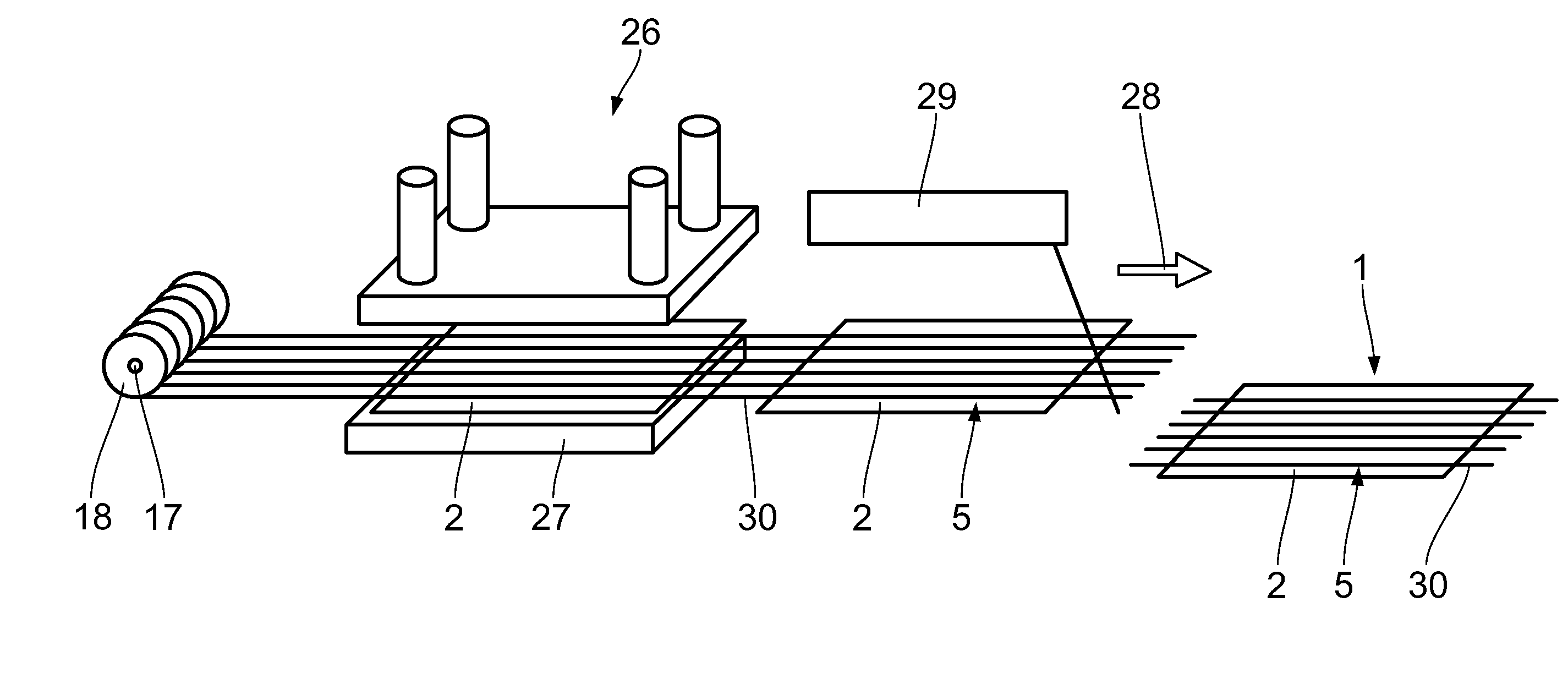
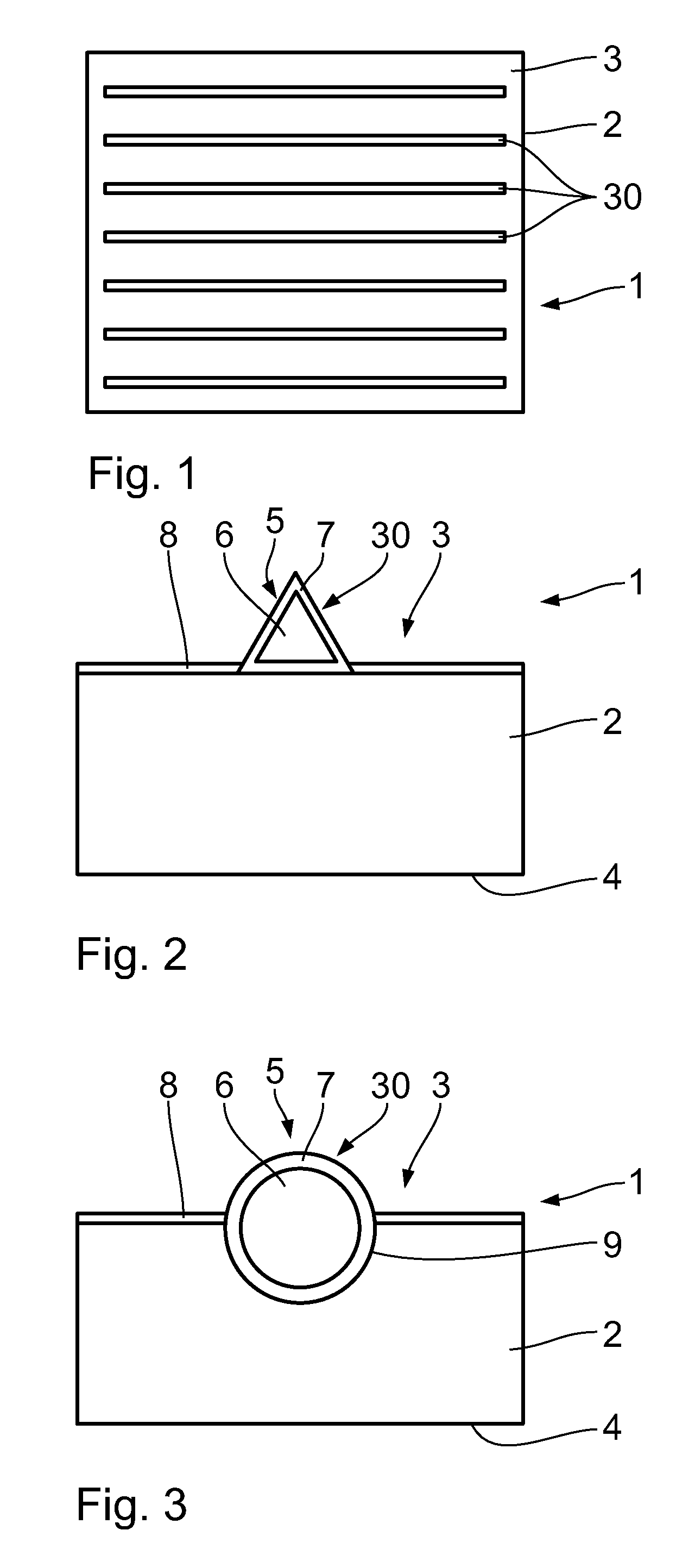
[0018]In the following, the invention is described with reference to FIGS. 1 and 2. A semiconductor component 1 especially designed as a solar cell comprises a semiconductor substrate 2 of a planar design, especially made of silicon, preferably p-doped silicon. The semiconductor substrate 2 can, however, also be made of another semiconductor material. The semiconductor substrate 2 exhibits a first side designed as a front side 3 and a second side designed as a rear side 4 lying opposite thereto.

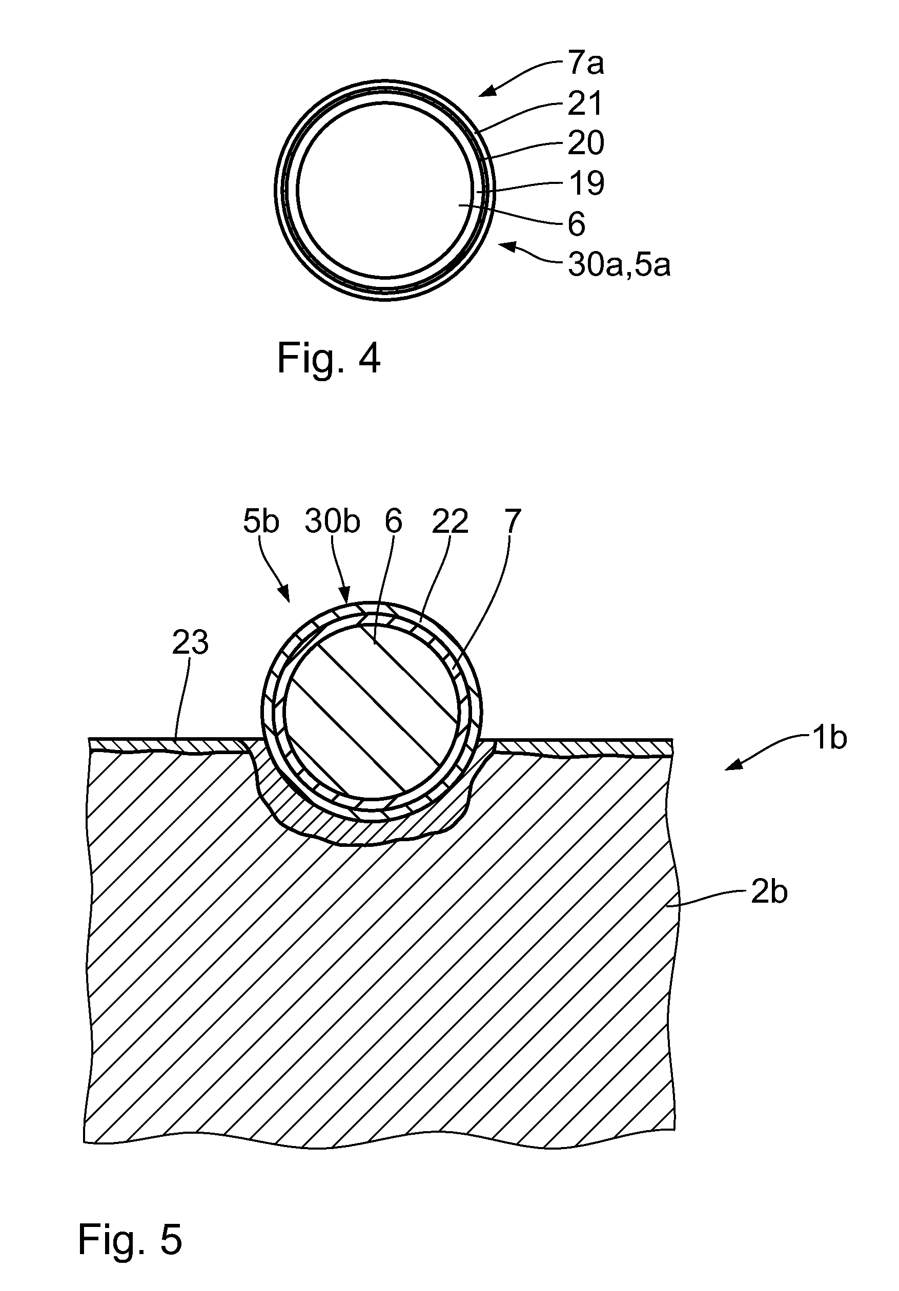
[0019]Moreover, the semiconductor component 1 comprises a contact structure 5 arranged on the front side 3. The contact structure 5 is formed by several metal wires 30, especially copper wires. The metal wires 30 of the contact structure 5 are especially arranged in parallel to each other. They each exhibit a metallic core 6, which is coated with a diffusion barrier 7. The core 6 is made of a material with a high specific conductance of at least 30 MS / m, especially at least 45 MS / m, preferabl...

second embodiment

[0032]In the following, the invention is described with reference to FIG. 3. Identical parts receive the same reference number as for the embodiment according to FIG. 2, reference to the description of which is hereby made. The difference to the embodiment according to FIG. 2 consists in that the contact structure 5 is arranged in a recess 9 in the semiconductor substrate 2 and / or in the protective layer 8. This increases the contact surface between the contact structure 5 and the semiconductor substrate 2. In this embodiment, the contact structure 5 preferably has a cross-section that is adapted to the recesses 9. Advantageously this is a round cross-section. In the area of the recess 9 the semiconductor substrate 2 preferably exhibits a higher doping with a dopant, especially phosphorous or boron.

[0033]The recess exhibits a depth which preferably corresponds to the radius of the wire 30. The wire 30 is thus arranged in the recess 9 with at least 30%, especially at least 40%, espec...

fourth embodiment

[0041]The contact structure 5b can, of course, also be used on the rear side 4 of a p-doped semiconductor substrate 2; especially the combination of a rear-side contact with a contact structure 5b and the semiconductor component 1 according to one of the previous embodiments is conceivable.


PUM


Abstract

A semiconductor component, especially a solar cell comprises a semiconductor substrate of a planar design having a first side and a second side lying opposite thereto, at least one contact structure arranged on at least one side of the semiconductor substrate, the at least one contact structure exhibiting a diffusion barrier to prevent the diffusion of ions from the contact structure into the semiconductor substrate.

Description

FIELD OF THE INTENTION[0001]The invention relates to a semiconductor component, a semiconductor module with at least two semiconductor components and a method for manufacturing such a semiconductor component.BACKGROUND ART[0002]Solar cells normally have a front side and a rear side, with a contact structure being applied on at least one of the two sides. The contact structure typically has a width of at least 100 μm, while its thickness is only about 10 to 15 μm. A greater width of the contact structure leads to a reduction in efficiency because of the increased shading that results. Conversely, a decrease of the width of the contact structure leads to an increase in the line resistances of the contact structure.SUMMARY OF THE INVENTION[0003]The invention is therefore based on the object of creating a semiconductor component with an improved contact structure. The invention is also based on the object of providing a method for manufacturing such a semiconductor component.[0004]Said ...

Claims


Application Information

Patent Timeline
Patent Type & Authority Applications(United States)
IPC IPC(8): H01L31/00H01L21/768
CPCH01L31/022425Y02E10/547H01L31/068
Inventor KRAUSE, ANDREASKUTZER, MARTINHEEMEIER, MICHAELFULLE, ALEXANDERNEUHAUS, HOLGER
Owner SOLARWORLD IND GMBH
Why Eureka
Try Eureka