

Active materials for photoelectric devices and devices that use the materials
a photoelectric device and active material technology, applied in the direction of photovoltaic energy generation, semiconductor devices, solid-state devices, etc., can solve the problems of inability to exceed the product maximum total power generated by a pv device, difficult and expensive production, and inability to efficiently crystalline-based devices, especially of large surface area, to achieve the effect of increasing the total power of the device, increasing the cost of production, and improving the stability
- Summary
- Abstract
- Description
- Claims
- Application Information
AI Technical Summary
Benefits of technology
Problems solved by technology
Method used
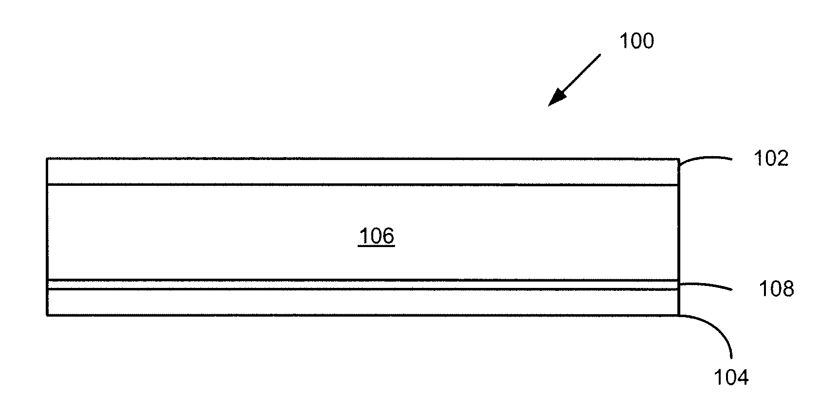
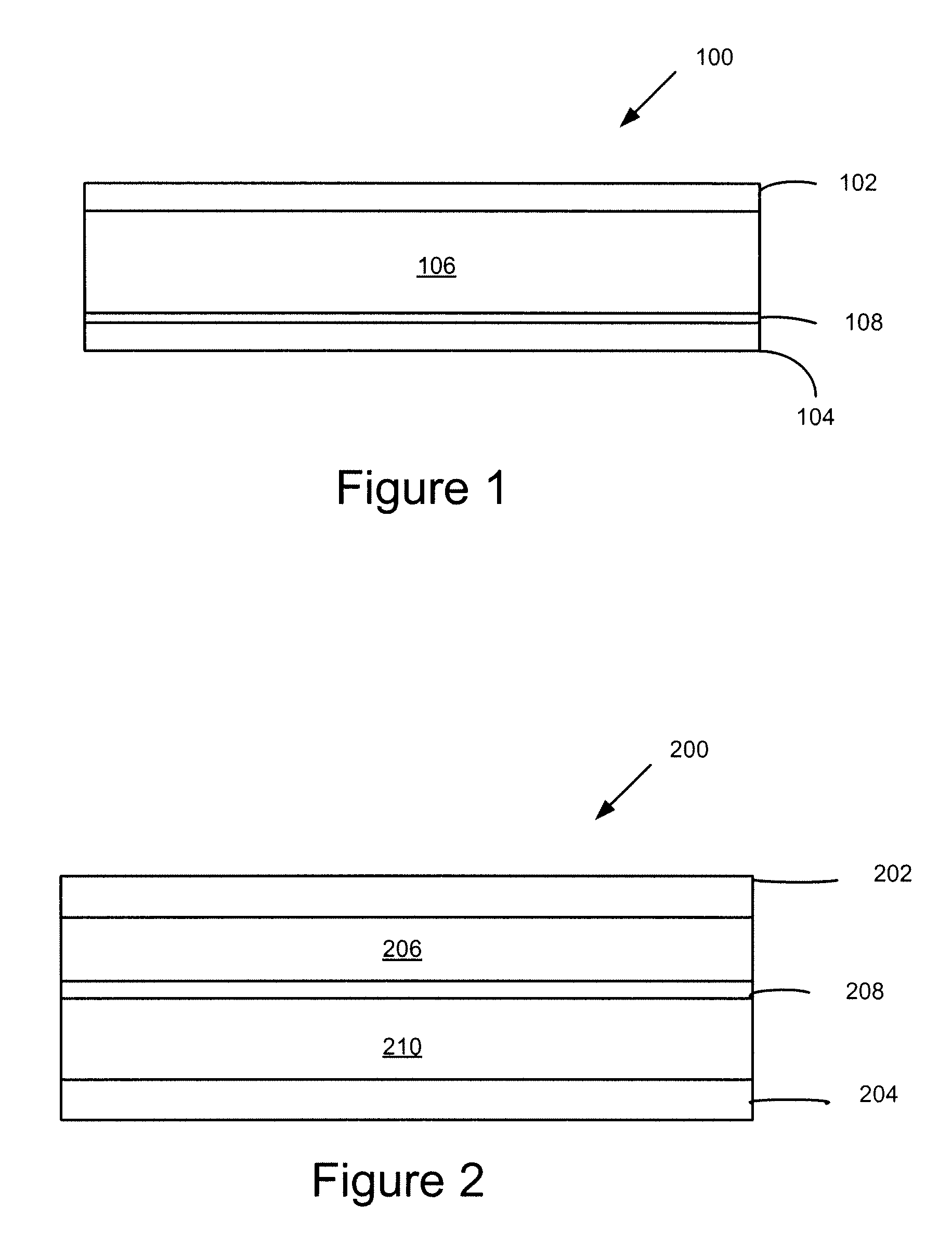
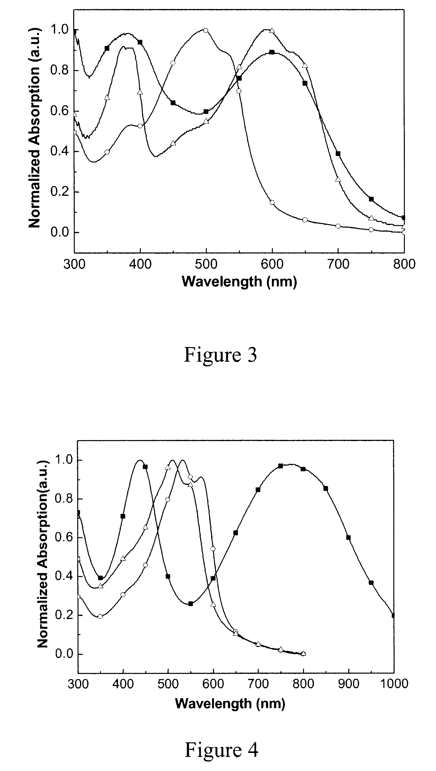
Image

Examples
example 1
Synthesis of 2,6-bis(trimethylstannyl)-4,8-didodecyloxy-benzo[1,2-b:4,5-b′]dithiophene
[0069]4,8-Dihydrobenzo[1,2-b:4,5-b′]dithiophen-4,8-dion, which is synthesized as the method published by Beimling [Chem. Ber. 1986; (119) 3198-3203.], Zinc powder (2.86 g, 44 mmol), and 60 ml of water were put into a 250 ml flask, then 12 g of NaOH was added. The mixture was well stirred and heated to reflux for one hour. Then, 1-bromo-dodecane (15 g, 60 mmol) and a catalytic amount of tetrabutyl ammonium bromide were added into the flask. The reactant was refluxed for 6 hours and poured into cold water, and extracted by 200 ml of diethyl ether for two times. The ether layer was dried over anhydrous MgSO4. After removing solvent, the crude product was purified by recrystallization from ethyl alcohol for two times. 9.26 g of 4,8-didodecyloxy-benzo[1,2-b; 3,4-b]dithiophene, was obtained as colorless crystal. 1H NMR (CDCl3): 7.66 (d, 2H), 7.47 (d, 2H), 4.26 (t, 4H), 1.87 (quintuple, 4H), 1.53 (m, 4H),...
example 2
Synthesis of Poly[4,8-didodecyloxy-benzo[1,2-b; 3,4-b]dithiophene-2,6-diyl]-Co-[2,3-diphenylquinoxaline-5,8-diyl]
[0073]5,8-dibromo-2,3-diphenylquinoxaline (0.44 g, 1 mmol, prepared according to Chen [J. Am. Chem. Soc., 2006, (128) 10992-10993]), 2,6-bis(trimethyltin)-4,8-didodecyloxy-benzo[1,2-b;3,4-b]-dithiophene, and 50 ml of toluene were put into a two-necked flask with oil bath. The solution was flushed with argon for 10 minutes, then 20 mg of Pd(PPh3)4 was added into the flask. The solution was flushed again for 20 minutes. The oil bath was heated to 110° C. carefully, and the reactant was stirred for 16 hours at this temperature under argon atmosphere. Then, the reactant was cooled to room temperature and the polymer was precipitated by addition of 100 ml methanol, and filtered through a Soxhlet thimble, which was then subjected to Soxhlet extraction with methanol hexane, and chloroform. The polymer was recovered as a solid sample from the chloroform fraction by rotary evapora...
example 3
Synthesis of Poly-2,6-(4,8-didodecyloxy-benzo[1,2-b; 3,4-b]dithiophene)
[0074]The procedure of example 2 was followed, except that 0.71 g of 2,6-dibromo-4,8-didodecyloxy-benzo[1,2-b; 3,4-b]dithiophene was used in stead of 5,8-dibromo-2,3-diphenylquinoxaline.
PUM
| Property | Measurement | Unit |
|---|---|---|
| Structure | aaaaa | aaaaa |
Abstract
Description
Claims
Application Information