Method for producing semiconductor laser, semiconductor laser, optical pickup, and optical disk drive

a technology of semiconductor lasers and optical pickups, applied in semiconductor lasers, record information storage, instruments, etc., can solve the problems of many methods of related art, nitride-based iii-v compound semiconductors, and many problems, so as to prevent light absorption and local heat generation, reduce waveguide loss, and efficiently utilize

Inactive Publication Date: 2010-04-01
SONY CORP
View PDF10 Cites 7 Cited by
  • Summary
  • Abstract
  • Description
  • Claims
  • Application Information

AI Technical Summary

Benefits of technology

[0026]In the above embodiments, a mask of an insulating film is formed on a nitride-based III-V compound semiconductor substrate at least near a position where an edge window structure is to be formed, and an active layer is grown in a region not covered by the mask. Because the diffusion distance of indium is significantly smaller than that of gallium, the indium content of the active layer is lower near the position where the edge window structure is to be formed than in other regions. Unlike in the related art, therefore, the edge window structure can be formed without forming a recess on the substrate. In addition, an appropriately selected mask shape prevents formation of steep steps in the nitride-based III-V compound semiconductor layer including the active layer, thus suppressing waveguide loss. In addition, no surface level appears because the edge window structure can be formed without etching the portion of the semiconductor layer forming the edge window structure by RIE, thus preventing light absorption and local heat generation during laser operation. In addition, the area of the nitride-based III-V compound semiconductor substrate can be efficiently utilized because two or more laser chip regions are defined between two adjacent second regions.
[0027]In addition, a pad electrode is formed in a region on the side of a laser stripe facing away from the mask so as to be electrically connected to the laser stripe. This prevents, for example, breakage of the pad electrode at a step. Specifically, a recess is formed above the mask after the growth of the nitride-based III-V compound semiconductor layer. If the pad electrode is formed in a region on the side of the laser stripe facing the mask, the pad electrode may be, for example, broken at a step in the recess above the mask. In contrast, because the surface in the region on the side of the laser stripe facing away from the mask is substantially flat, the pad electrode can be formed in the substantially flat region without the risk of, for example, breakage of the pad electrode at a step.
[0028]According to the above embodiments, it is possible to provide a semiconductor laser using a nitride-based III-V compound semiconductor in which an edge window structure can be easily formed, in which waveguide loss can be suppressed, and in which light absorption and local heat generation during laser operation can be suppressed. In addition, a larger number of semiconductor lasers can be produced from a single nitride-based III-V compound semiconductor substrate. In addition, the superior semiconductor laser can be used as a light source for an optical pickup to provide an optical disk drive with high performance.

Problems solved by technology

As described above, the methods of the related art for forming an edge window structure in a semiconductor laser using a nitride-based III-V compound semiconductor have many problems.

Method used


Image

  • Method for producing semiconductor laser, semiconductor laser, optical pickup, and optical disk drive
  • Method for producing semiconductor laser, semiconductor laser, optical pickup, and optical disk drive
  • Method for producing semiconductor laser, semiconductor laser, optical pickup, and optical disk drive

Examples


first embodiment

2. First Embodiment

Semiconductor Laser and Method for Producing Semiconductor Laser

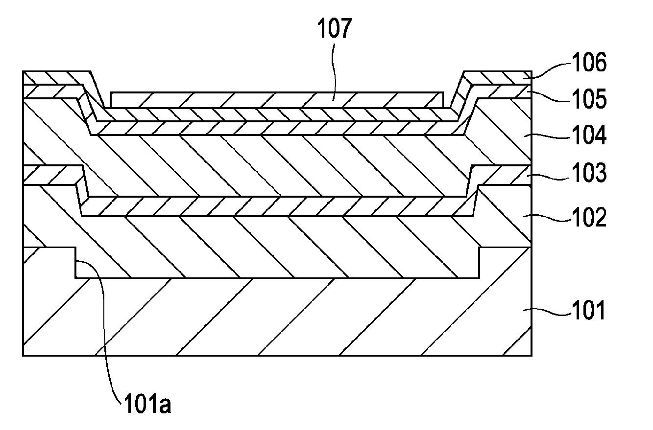
[0104]FIG. 8 shows an n-type GaN substrate used as a substrate in a method for producing a GaN-based semiconductor laser according to the first embodiment. The details of the n-type GaN substrate and a method for producing the substrate are disclosed in Patent Document 12.

[0105]As shown in FIG. 8, an n-type GaN substrate 11 includes first regions 11a formed of single-crystal GaN and second regions 11b formed of GaN and periodically arranged in parallel between the first regions 11a so as to extend linearly in a striped pattern.

[0106]The second regions 11b are formed of polycrystals, single crystals slightly inclined with respect to those of the first regions 11a, or single crystals inverted along the c-axis with respect to those of the first regions 11a. The first regions 11a have a first average dislocation density, whereas the second regions 11b have a second average dislocation density higher than ...

second embodiment

3. Second Embodiment

Semiconductor Laser and Method for Producing Semiconductor Laser

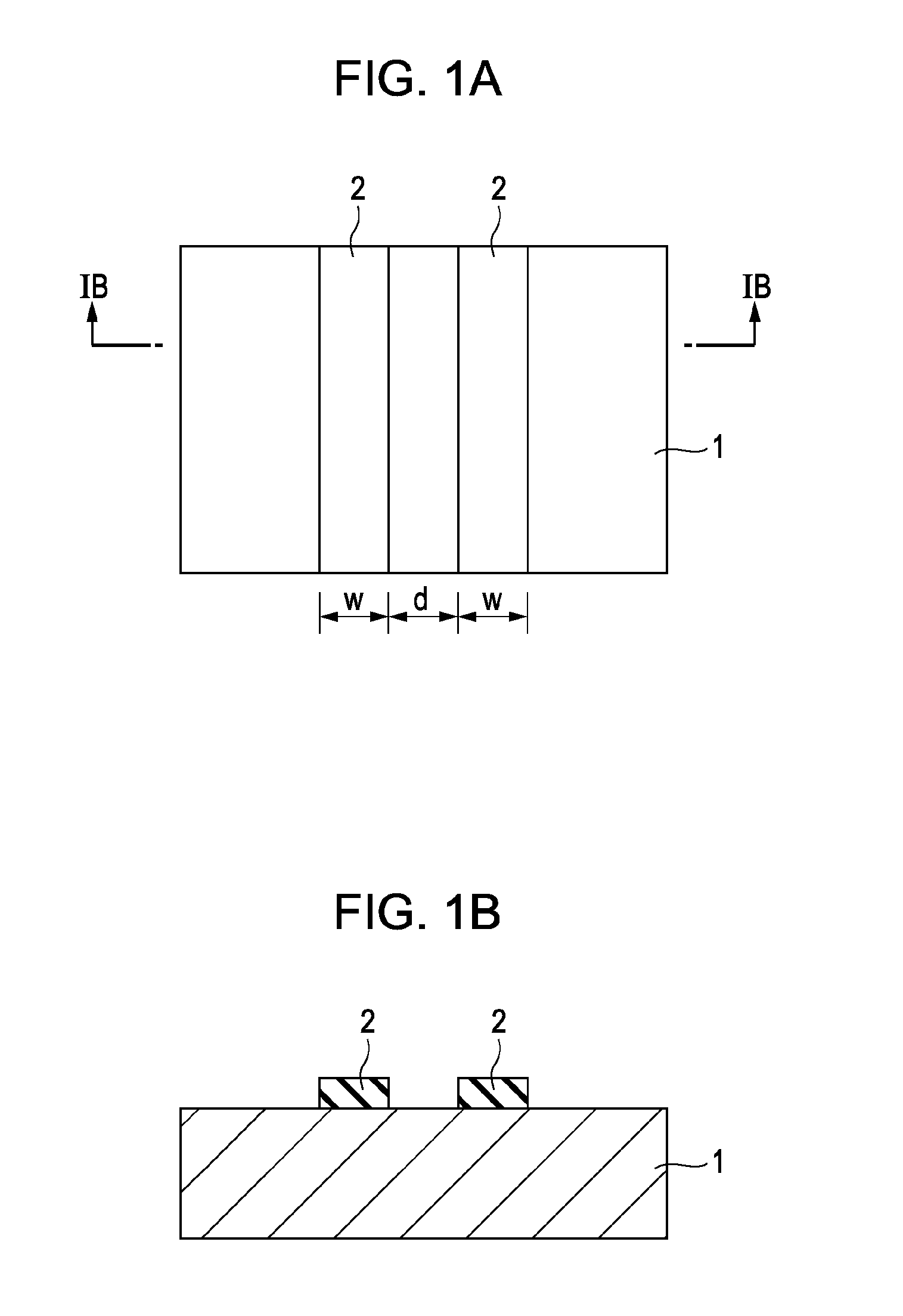
[0165]The second embodiment differs from the first embodiment in the shape and positions of the insulating film masks 16. In other respects, the second embodiment is similar to the first embodiment.

[0166]In the second embodiment, first, as shown in FIG. 14, an elongated insulating film mask 16 with a constant width is formed on one side of each ridge-stripe forming position 15 on the n-type GaN substrate 11, specifically, on the side opposite the center line of the first region 11a between each two adjacent second regions 11b, over the length of the resonator.

[0167]An edge of the insulating film mask 16 opposite the ridge-stripe forming position 15 agrees with an edge of the ridge-stripe forming position 15 in the center in the resonator length direction and is separated from the ridge-stripe forming position 15 at an interval w1 over the distance d1 from the resonator-edge forming positions 13 and 1...

third embodiment

4. Third Embodiment

Semiconductor Laser and Method for Producing Semiconductor Laser

[0172]The third embodiment differs from the first and second embodiments in the shape and positions of the insulating film masks 16. In other respects, the third embodiment is similar to the first embodiment.

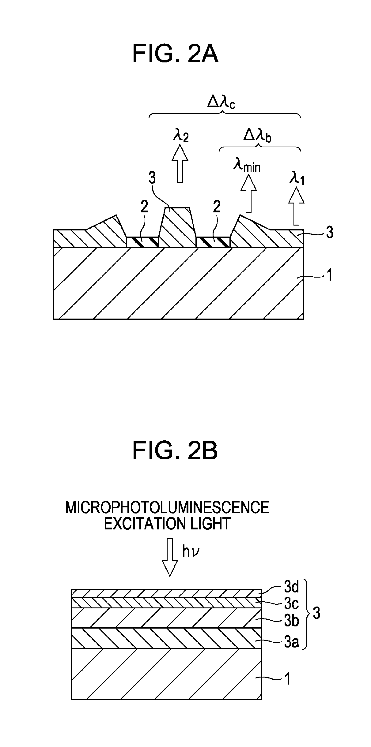
[0173]In the third embodiment, first, as shown in FIG. 15, the insulating film masks 16 used in the second embodiment are symmetrically formed on both sides of each ridge-stripe forming position 15 on the n-type GaN substrate 11. For example, d1 is 20 μm, d2 is 50 μm, the width of the insulating film masks 16 is 5 μm, and the interval w1 between the insulating masks 16 and the ridge-stripe forming position 15 is 3 to 20 μm, although they are not limited.

[0174]Next, as in the first embodiment, the GaN-based semiconductor layer 25 forming a laser structure is grown on the n-type GaN substrate 11 with the insulating film masks 16 by, for example, MOCVD. For the active layer 19, which contains indium ...


PUM

PropertyMeasurementUnit
bandgap energyaaaaaaaaaa
widthaaaaaaaaaa
widthaaaaaaaaaa

Abstract

A method for producing a semiconductor laser having an edge window structure includes the steps of forming masks of insulating films on a nitride-based III-V compound semiconductor substrate including first regions and second regions periodically arranged in parallel therebetween; and growing a nitride-based III-V compound semiconductor layer in a region not covered by the masks. The first region between each two adjacent second regions has two or more positions, symmetrical with respect to a center line thereof, where laser stripes are to be formed. The masks are formed on one or both sides of each of the positions where the laser stripes are to be formed at least near a position where edge window structures are to be formed such that the masks are symmetrical with respect to the center line. The nitride-based III-V compound semiconductor layer includes an active layer containing at least indium and gallium.

Description

BACKGROUND OF THE INVENTION[0001]1. Field of the Invention[0002]The present invention relates to methods for producing semiconductor lasers, semiconductor lasers, optical pickups, and optical disk drives. More specifically, the present invention is suitable for application to, for example, ridge-stripe semiconductor lasers with an edge window structure using nitride-based III-V compound semiconductors and optical pickups and optical disk drives using such semiconductor lasers as light sources.[0003]2. Description of the Related Art[0004]To increase the maximum optical output of a semiconductor laser, it is effective to introduce an edge window structure where a window transparent to light emitted from an active layer is provided at an edge of a resonator.[0005]For GaInP-based red light-emitting semiconductor lasers, it is effective to form an edge window structure by diffusing zinc atoms into a semiconductor layer forming a laser structure near a position corresponding to an edge of...

Claims


Application Information

Patent Timeline
Patent Type & Authority Applications(United States)
IPC IPC(8): G11B7/00H01L33/00H01S5/16H01S5/028
CPCB82Y20/00H01S5/16H01S5/34333H01S5/2275H01S5/2277H01S5/168
Inventor KODA, RINTAROKURAMOTO, MASARUNAKAYAMA, EIJIFUJIMOTO, TSUYOSHI
Owner SONY CORP
Why Eureka
Try Eureka