

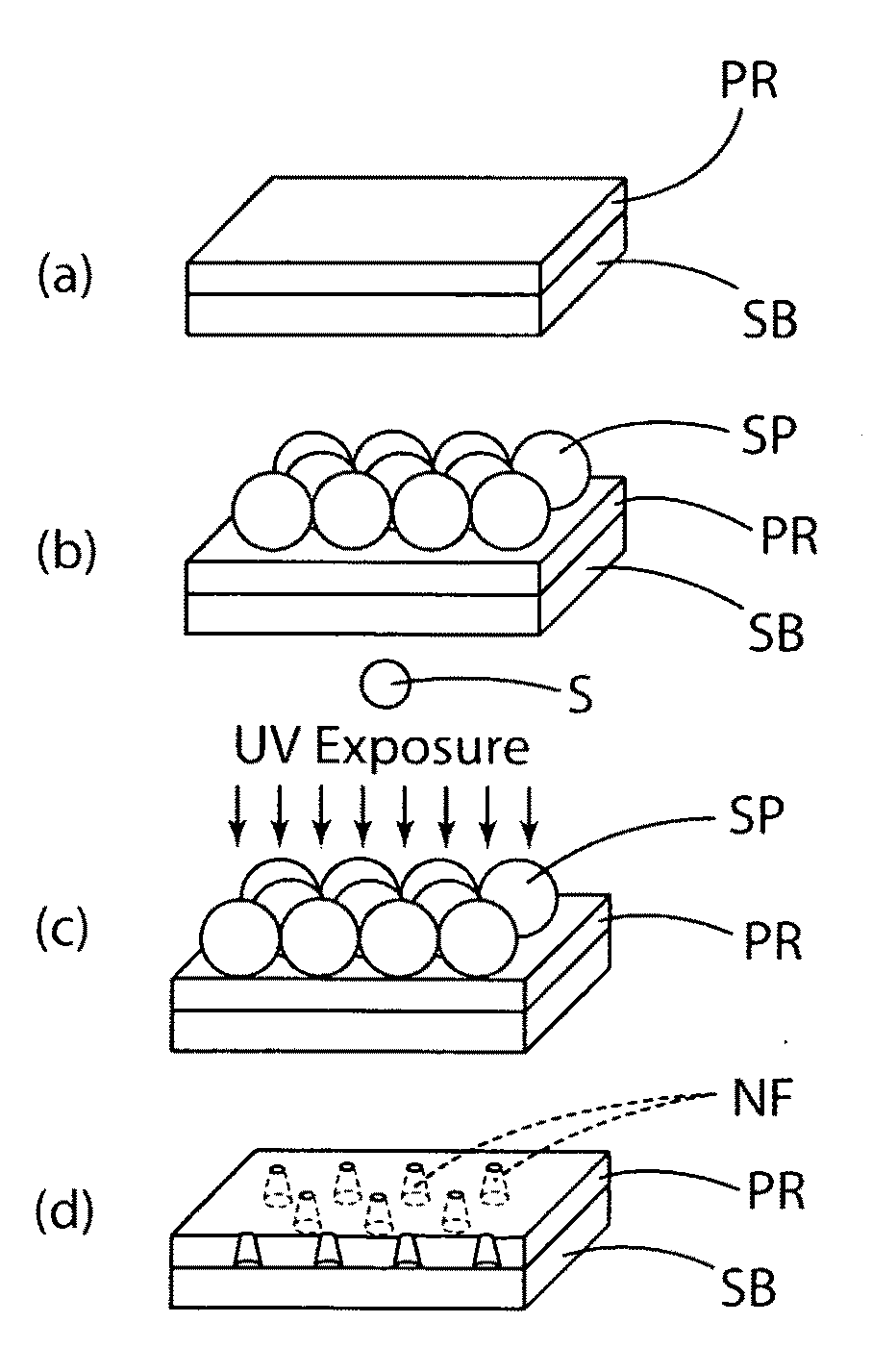
Process for formation of highly uniform arrays of nano-holes and nano-pillars
a nano-hole and nano-pillar technology, applied in the field of photolithography methods, can solve the problems of slow or expensive fabrication over large areas, limitations of conventional photolithography methods, and inability to meet the small dimension requirements of many applications, and achieve the effect of low cost and high throughpu
- Summary
- Abstract
- Description
- Claims
- Application Information
AI Technical Summary
Benefits of technology
Problems solved by technology
Method used
Image

Examples
example 1
EXAMPLE 1
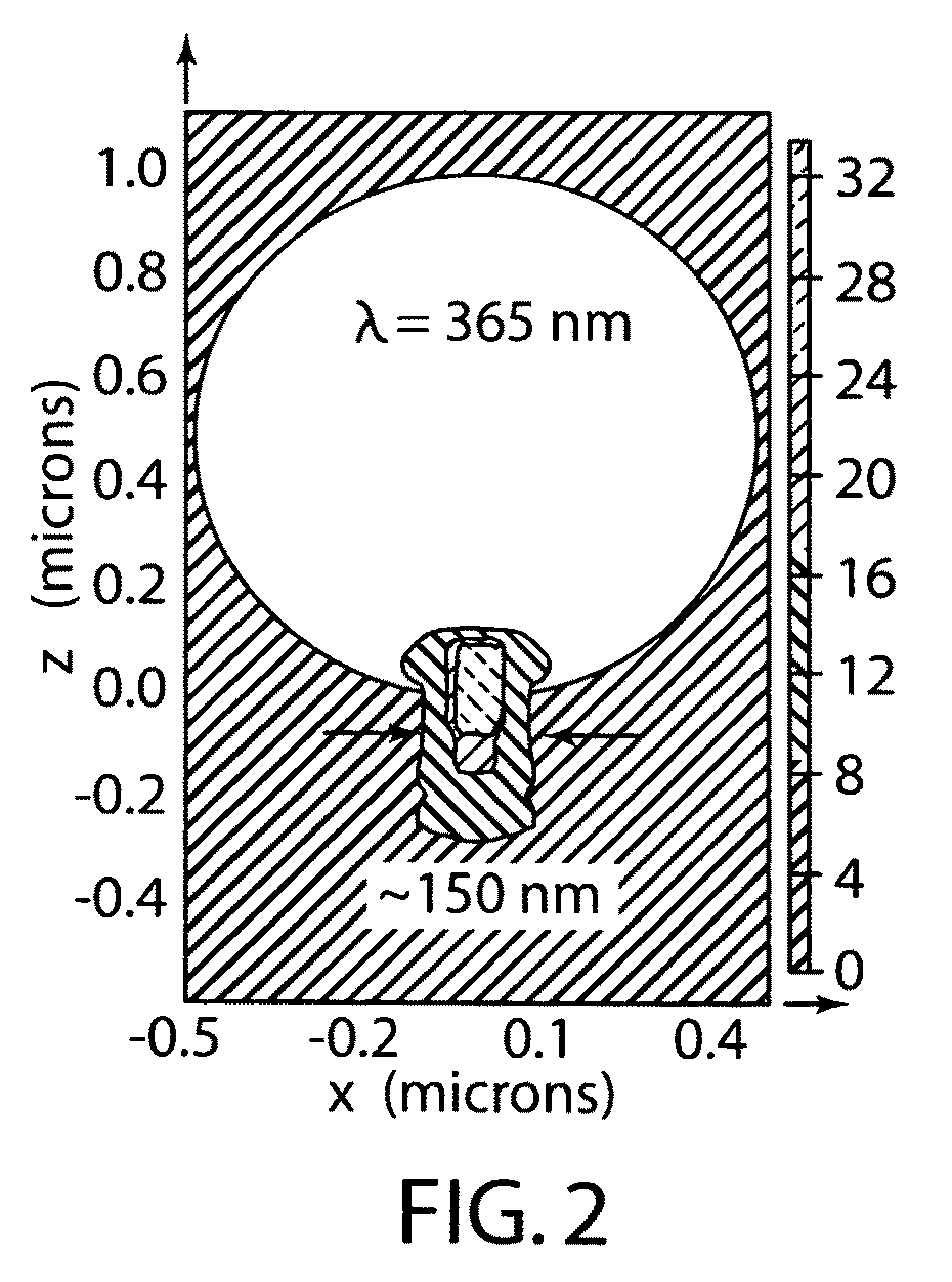
[0036]GaAs substrates were prepared with two kinds of commonly used photoresists; namely, AZ 5214-E and Shipley 1805 available from Clariant Corp. and Shipley Co. respectively. The photoresists were applied to a thickness of 1 um and 500 nm, respectively. All process steps were performed in a class 100 clean-room. Two types of spheres, silica and polystyrene (PS), were used to form hexagonal close packing (HCP) arrays on top of the photoresists. A 10 wt. % aqueous suspension of transparent silica or polystyrene spheres of 0.97 um diameter. The silica or PS microspheres both were purchased from Bangs Laboratory, Inc. The silica and PS microspheres had uniform diameters of about 0.97 micron (typical size standard deviation is 5-10%). Before usage, the aqueous suspension was diluted by deionized water down to 0.1 wt. % for both types of the spheres. Higher concentration of the spheres formed multi-layers of microspheres and a low concentration would not be sufficient to form ...
example 2
EXAMPLE 2
[0044]The basic method flow for this Example is shown in shown in FIGS. 8a; 8b; 8c, 8c′; and 8d, 8d′ where FIGS. 8c, 8c′ and 8d, 8d′ illustrate the processing using a positive and negative photoresist, respectively. Photoresist PR was spun on the substrate SB. Positive photoresist (Shipley 1805) was commercially available from Shipley Co. Negative photoresist (Ma-N 1405) was commercially available from MicroChem Corp. The positive photoresist was treated with developer AZ-300 MIF to render it hydrophilic enough to permit formation of a particle monolayer using an aqueous dispersion of microspheres. A monolayer of micro-spheres SP was formed on top of the photoresist, FIG. 8a, as described in Example 1. Silica micro-spheres of 1 μm diameter were bought from Bangs Lab. The sample with the monolayer of micro-spheres on the photoresist was exposed with a conventional Quintel exposure instrument with broadband wavelength centered about 400 nm, FIG. 8b. The micro-spheres were re...
PUM
| Property | Measurement | Unit |
|---|---|---|
| diameter | aaaaa | aaaaa |
| wavelength | aaaaa | aaaaa |
| hole diameter | aaaaa | aaaaa |
Abstract
Description
Claims
Application Information