

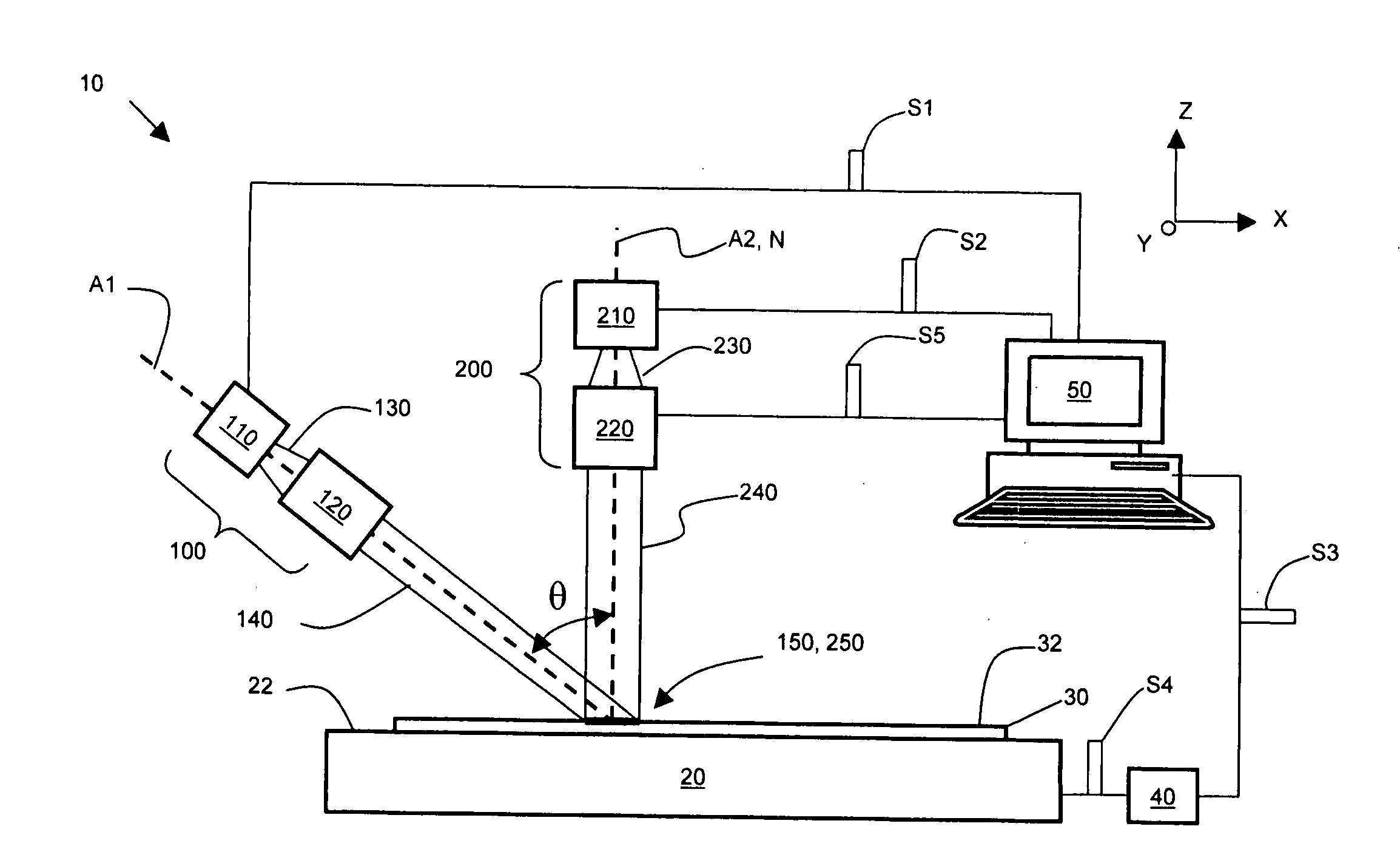
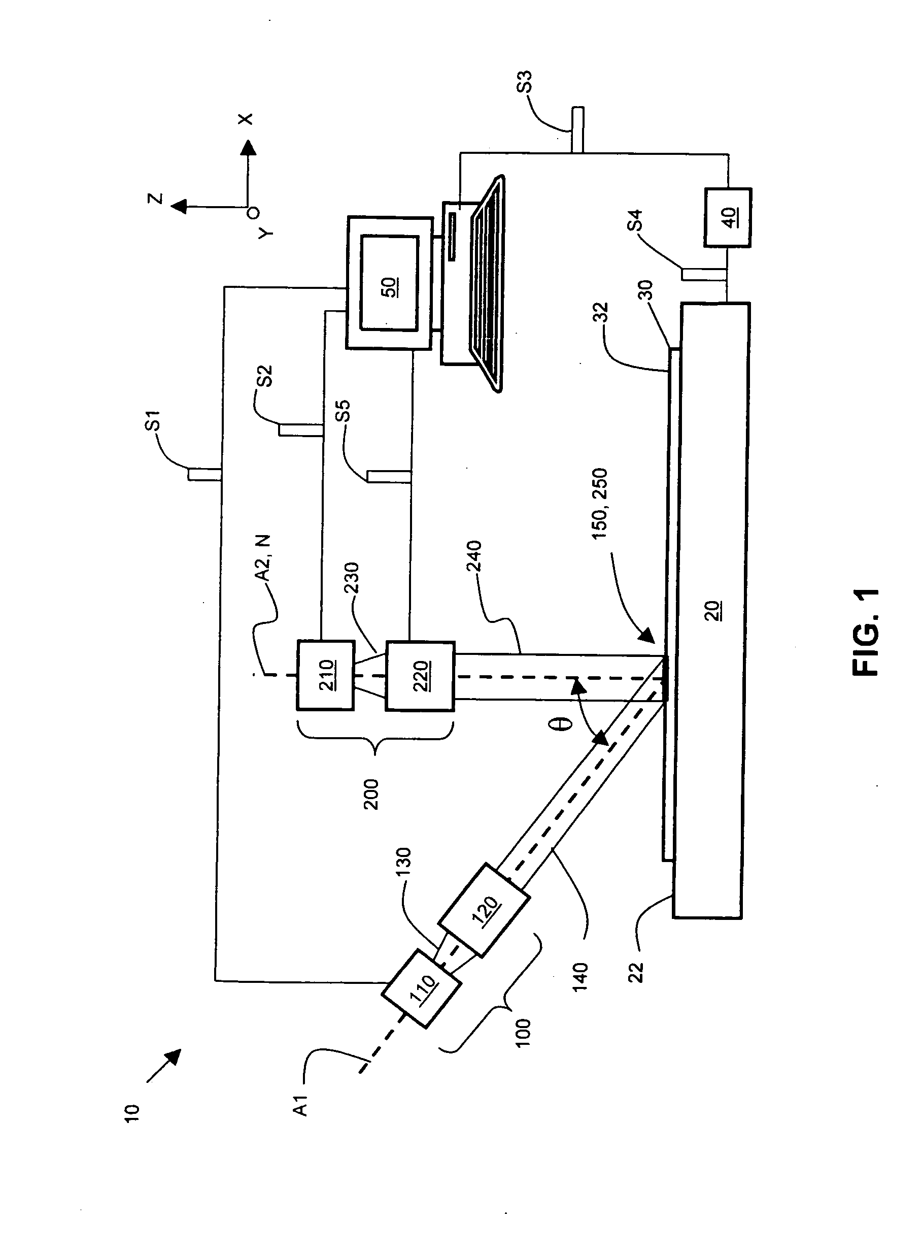
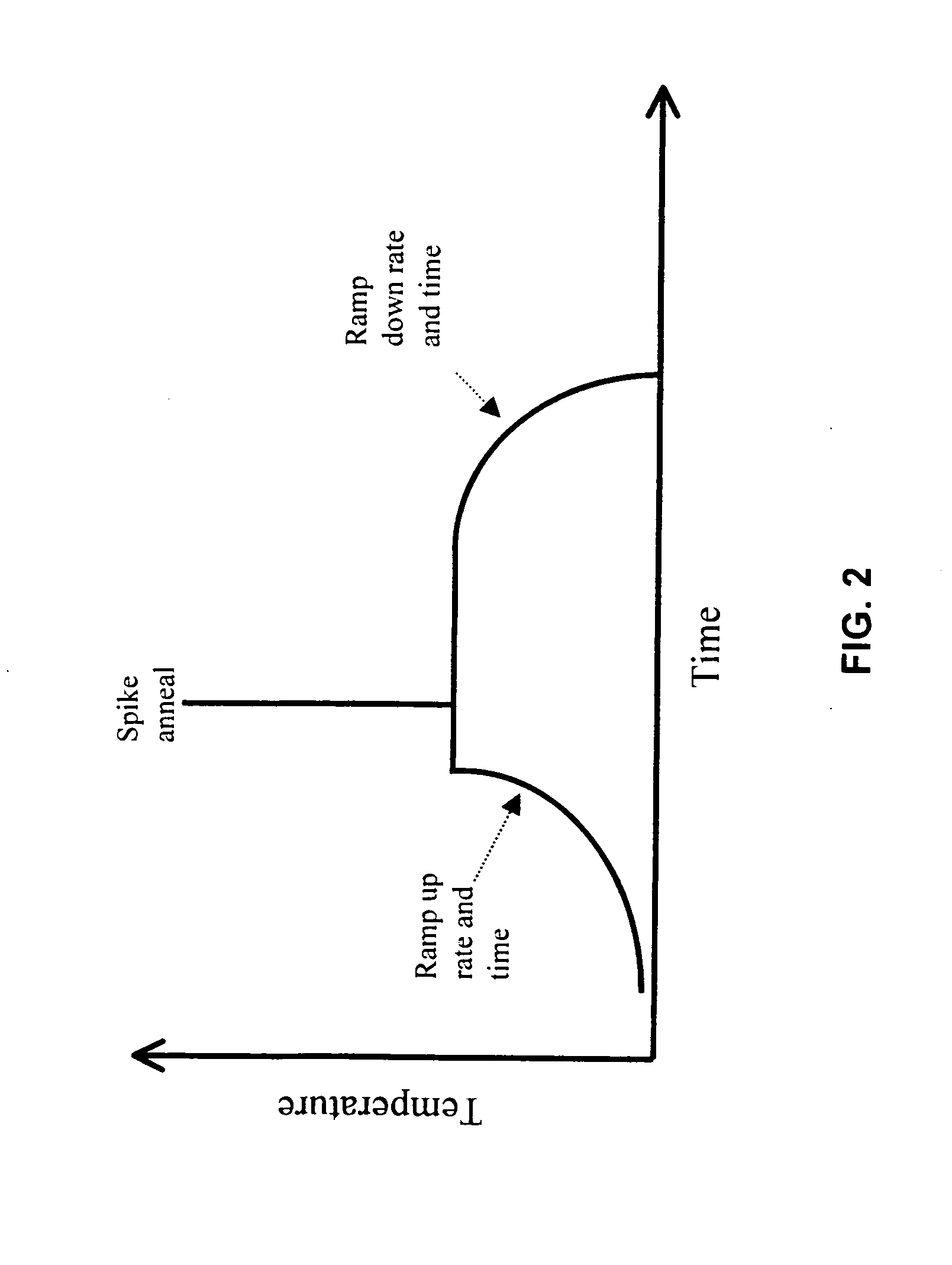
Thermal processing of substrates with pre- and post-spike temperature control
a technology of temperature control and substrate, applied in the field of substrate thermal processing, can solve the problems of thermal spike, uncontrolled stress in the substrate, light doped and undoped silicon may not significantly absorb, etc., and achieve the effect of improving the electronic performance of the substrate and reducing the accumulation of stress
- Summary
- Abstract
- Description
- Claims
- Application Information
AI Technical Summary
Benefits of technology
Problems solved by technology
Method used
Image

Examples
Embodiment Construction
Definitions and Overview
[0029]Before describing the present invention in detail, it is to be understood that this invention, unless otherwise noted, is not limited to specific substrate constructions, substrate materials, radiation sources, as such may vary. It is also to be understood that the terminology used herein is for the purpose of describing particular embodiments only, and is not intended to be limiting.
[0030]It must be noted that, as used in this specification and the appended claims, the singular forms “a”, “an” and “the” include both singular and plural referents unless the context clearly dictates otherwise. Thus, for example, reference to “beam” includes a plurality of beams as well as a single beam, reference to “a wavelength” includes a range or plurality of wavelengths as well as a single wavelength, reference to “a region” includes a combination of regions as well as single region, and the like.
[0031]In describing and claiming the present invention, the following ...
PUM
| Property | Measurement | Unit |
|---|---|---|
| temperatures | aaaaa | aaaaa |
| peak temperature | aaaaa | aaaaa |
| dwell time | aaaaa | aaaaa |
Abstract
Description
Claims
Application Information