

Semiconductor devices having faceted silicide contacts, and related fabrication methods
a technology of silicide contacts and semiconductors, applied in the direction of semiconductor devices, bulk negative resistance effect devices, electrical appliances, etc., can solve the problems of high contact resistance, and inability to meet the requirements of the minimum spacer siz
- Summary
- Abstract
- Description
- Claims
- Application Information
AI Technical Summary
Benefits of technology
Problems solved by technology
Method used
Image

Examples
first embodiment
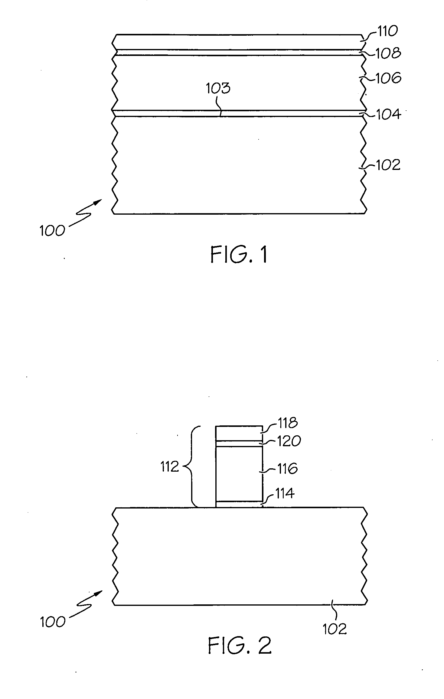
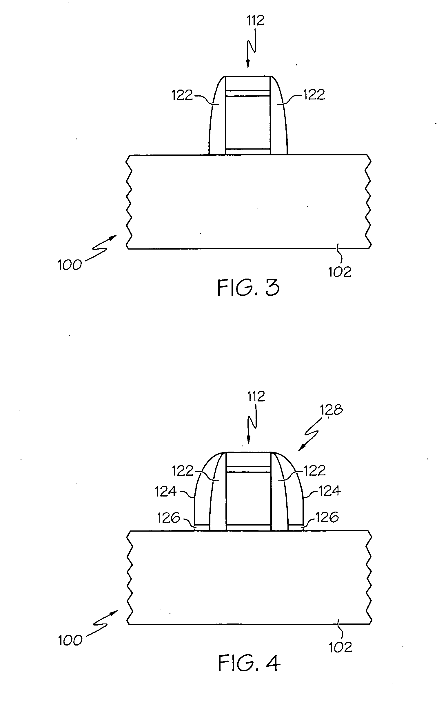
[0028]FIGS. 6-11 are cross sectional views that illustrate the fabrication of a semiconductor device 200 in accordance with a The following description assumes that a device structure as shown in FIG. 5 has already been formed and provided. In this regard, although other fabrication steps or sub-processes may be performed after formation of the device structure depicted in FIG. 5, this example continues with an etching step, which preferably employs an anisotropic etch technique. In accordance with this embodiment, gate structures 128 are used as a hard etch mask to form recesses 202 in the semiconductor material 102 adjacent to gate structures 128 (FIG. 6). Recesses 202 can be anisotropically etched using any suitable etchant or chemistry, such as chlorine or HBr / O2 chemistry. This etching step is controlled to form recesses 202 having the desired depth for the given device structure. Notably, recesses 202 are self-aligned with disposable spacers 124. As used herein, self-aligned ...
second embodiment
[0038]FIGS. 12-14 are cross sectional views that illustrate the fabrication of a semiconductor device 300 in accordance with a This embodiment relates to the fabrication of a PMOS transistor device. The following description assumes that a device structure as shown in FIG. 6 has already been formed and provided. In this regard, although other fabrication steps or sub-processes may be performed after formation of the device structure depicted in FIG. 6, this example continues by at least partially filling recesses 202 with a filler semiconductor material 302, to form facet-shaped semiconductor regions 304 in recesses 202 (FIG. 12 and FIG. 13). During this step, filler semiconductor material 302 may be an undoped semiconductor material or an in situ doped semiconductor material, as described above for semiconductor device 200. In this embodiment, filler semiconductor material 302 is a stress-inducing semiconductor material that is formed by selectively epitaxially growing the materia...
third embodiment
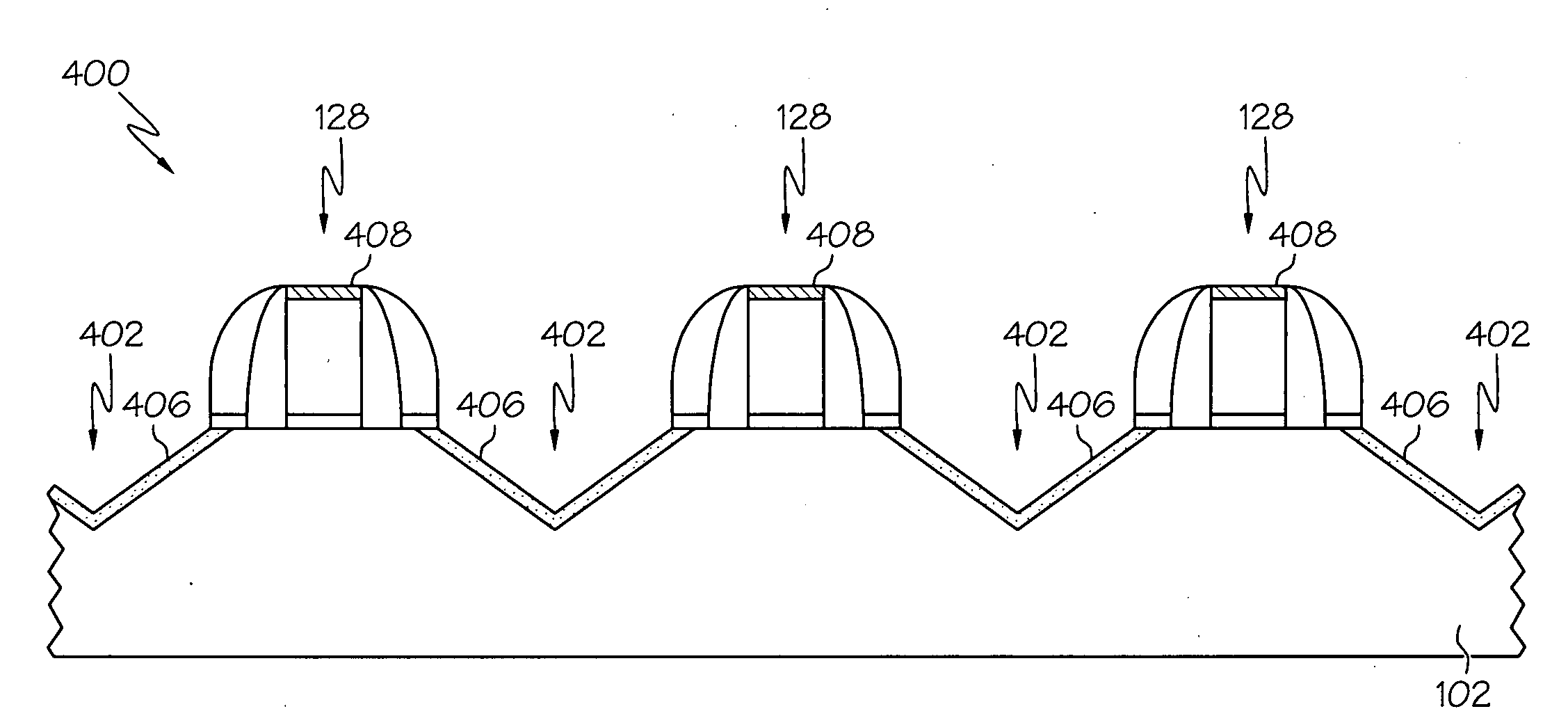
[0043]FIGS. 15 and 16 are cross sectional views that illustrate the fabrication of a semiconductor device 400 in accordance with a This embodiment is applicable to PMOS and NMOS transistor devices, where semiconductor material 102 is oriented on its {100} plane or its {110} plane. The following description assumes that a device structure as shown in FIG. 5 has already been formed and provided. In this regard, although other fabrication steps or sub-processes may be performed after formation of the device structure depicted in FIG. 5, this example continues with an etching step, which preferably employs a suitable wet etch chemistry that attacks the different crystal planes at different rates. In accordance with this embodiment, gate structures 128 are used as a hard etch mask to form facet-shaped recesses 402 in the semiconductor material 102 adjacent to gate structures 128 (FIG. 15).
[0044]Facet-shaped recesses 402 can be etched using any suitable etchant or chemistry that etches t...
PUM
 Abstract
Description
Claims
Application Information