Air gap interconnects using carbon-based films

a carbon-based film and air gap technology, applied in the direction of basic electric elements, electrical equipment, semiconductor/solid-state device manufacturing, etc., can solve the problems of increased intra-line capacitance and cross-talk between closely spaced interconnect lines, affecting the effect, and difficult removal of sacrificial imds, etc., and achieve good electrical isolation properties

Inactive Publication Date: 2010-04-15
APPLIED MATERIALS INC
View PDF3 Cites 247 Cited by
  • Summary
  • Abstract
  • Description
  • Claims
  • Application Information

AI Technical Summary

Benefits of technology

[0010]Embodiments may further comprise: planarizing the non-conformal dielectric layer, wherein in the air gap area the air gaps are engulfed in the planarized non-conformal dielectric, and wherein planarizing the non-conformal dielectric layer in the exclusion area removes at least part of the non-conformal dielectric from the excl...

Problems solved by technology

This results in increased intra-line capacitance and cross-talk between the closely spaced interconnect lines.
One of the issues related to making air gap interconnects is the removal of a sacrificial inter-metal-dielectric (IMD), which is later substituted by a non-conformal chemical vapor deposition (CVD) die...

Method used


Image

  • Air gap interconnects using carbon-based films
  • Air gap interconnects using carbon-based films
  • Air gap interconnects using carbon-based films

Examples


Embodiment Construction

[0032]In the following description, various aspects of the present invention will be described, and various details set forth in order to provide a thorough understanding of the present invention. However, it would be apparent to those skilled in the art that the present invention may be practiced with only some or all of the aspects of the present invention, and the present invention may be practiced without the specific details. In other instances, well-known features are admitted or simplified in order not to obscure the present invention.

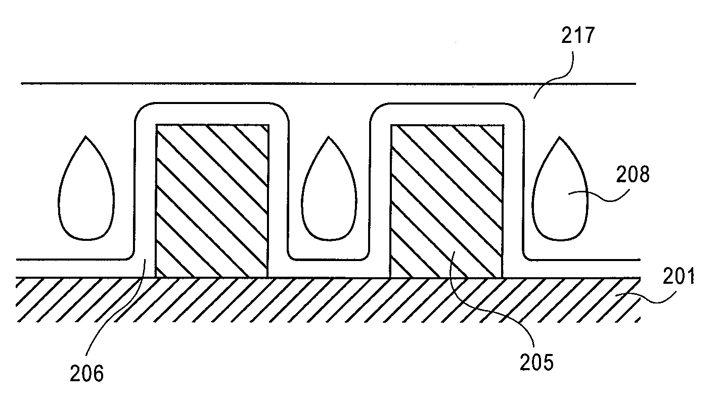
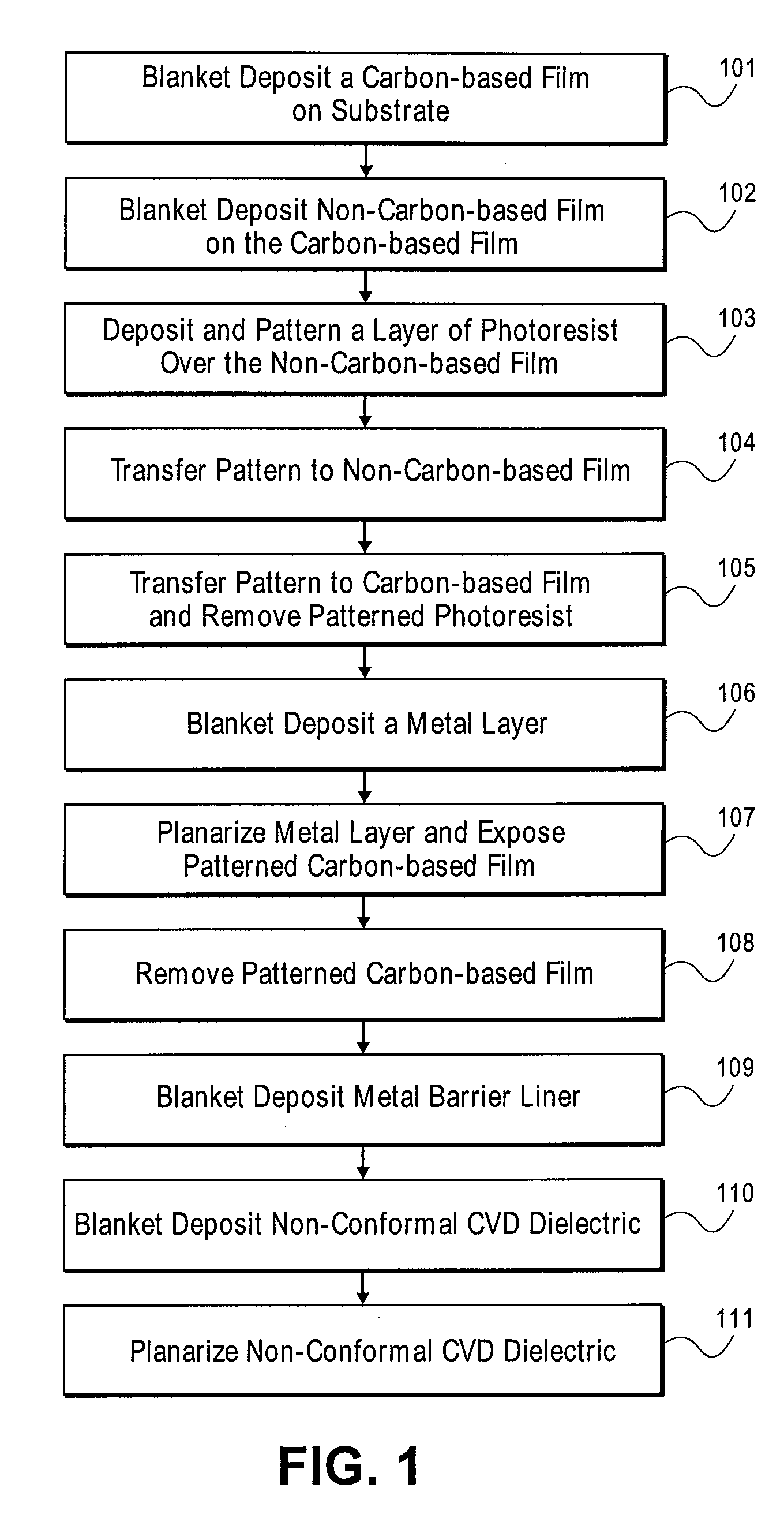
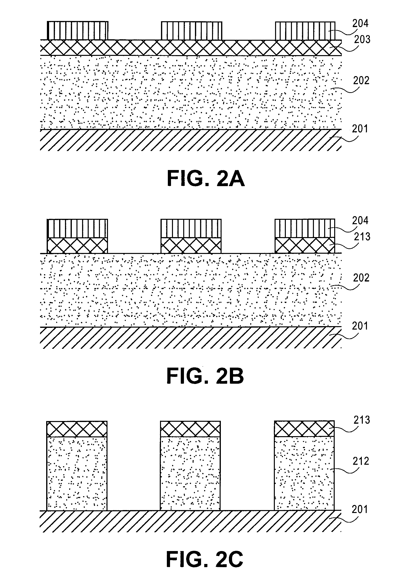
[0033]It should be understood that FIGS. 1A through 14F are merely illustrative and may not be drawn to scale. While certain exemplary embodiments have been described and shown in the accompanying drawings, it is to be understood that such embodiments are merely illustrative and not restrictive of the current invention, and that this invention is not restricted to the specific constructions and arrangements shown and described since modification...


PUM


Abstract

A method of forming an interconnect structure comprising: forming a sacrificial inter-metal dielectric (IMD) layer over a substrate, wherein the sacrificial IMD layer comprising a carbon-based film, such as amorphous carbon, advanced patterning films, porous carbon, or any combination thereof; forming a plurality of metal interconnect lines within the sacrificial IMD layer; removing the sacrificial IMD layer, with an oxygen based reactive process; and depositing a non-conformal dielectric layer to form air gaps between the plurality of metal interconnect lines. The metal interconnect lines may comprise copper, aluminum, tantalum, tungsten, titanium, tantalum nitride, titanium nitride, tungsten nitride, or any combination thereof. Carbon-based films and patterned photoresist layers may be simultaneously removed with the same reactive process. Highly reactive hydrogen radicals processes may be used to remove the carbon-based film and simultaneously pre-clean the metal interconnect lines prior to the deposition of a conformal metal barrier liner.

Description

BACKGROUND OF THE INVENTION[0001]1. Field of the Invention[0002]The present invention relates to electrical interconnect structures for interconnecting a plurality of devices, such as semiconductor devices. In particular, to methods of making interconnect structures having air gaps in the dielectric material between the interconnect lines of the interconnect structure.[0003]2. Discussion of Related Art[0004]The semiconductor industry is continually pursuing smaller and smaller geometries of the structures used in semiconductor devices. As the device geometries become smaller, more devices are fabricated into the same area of semiconductor substrate. Therefore, the number of interconnect lines in the same area of substrate must also increase, thus requiring that the spacing between the interconnect lines to also decrease in size. This results in increased intra-line capacitance and cross-talk between the closely spaced interconnect lines.[0005]In order to reduce intra-line capacitanc...

Claims


Application Information

Patent Timeline
IPC IPC(8): H01L21/4763
CPCH01L21/31144H01L21/76807H01L21/76813H01L21/76885H01L21/76834H01L21/76837H01L21/7682H01L21/76816H01L21/76811
Inventor NAIK, MEHUL
Owner APPLIED MATERIALS INC
Why Eureka
Try Eureka