Packaging struture for high power light emitting diode(LED) chip

a technology of led chip and packaging structure, which is applied in the direction of basic electric elements, electrical equipment, semiconductor devices, etc., can solve the problems of shortened service life of the chip, reduced production efficiency, and increased heat resistance, so as to improve production efficiency and manufacturing efficiency, facilitate mass production, and simplify manufacturing processes

Inactive Publication Date: 2010-04-22
BRILLIANT TECH
View PDF2 Cites 35 Cited by
  • Summary
  • Abstract
  • Description
  • Claims
  • Application Information

AI Technical Summary

Benefits of technology

[0012]The primary objective of the present invention lies in forming at least one containing slot for mounting a chip on the surface of a metal plate, opening two isolating slots on two external sides of the containing slot in converse directions, and embedding insulators in the isolating slots. The metal plate and the insulators are covered and combined with a cover plate, allowing a hollow slot and notches on the surface of the cover plate to correspond with the containing slot and the isolating slots to form a hollowness state. Then, the metal plate is cut on both sides along the free ends of the insulators so as to form electrode contacts with positive and negative electrodes, and the surface mount technology (SMT) can be adopted for assembly to sim

Problems solved by technology

1. There is no component installed in the insulator B for radiating heat produced from the chip A. Therefore, this may lead to disadvantages and problems of poor heat radiation or difficulty in heat dissipation when the chip A emits light, resulting in considerable increase of heat resistance, lower performance, or shortened service life of the chip A due to overheat.
2. The positive electrode pin C and the negative electrode pin D is electrically connected with a circuit board by insertion. This makes the overall height of the low-power LED unable to be reduced effectively; rather it will occupy some space. So it will not meet the requirement for thin products in design.
3. The light emitted from the chip A is liable to scattering, resulting in loss of light, this will lead to attenuation

Method used


Image

  • Packaging struture for high power light emitting diode(LED) chip
  • Packaging struture for high power light emitting diode(LED) chip
  • Packaging struture for high power light emitting diode(LED) chip

Examples


Embodiment Construction

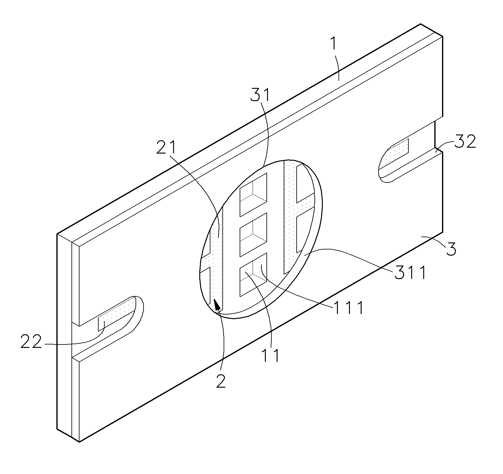
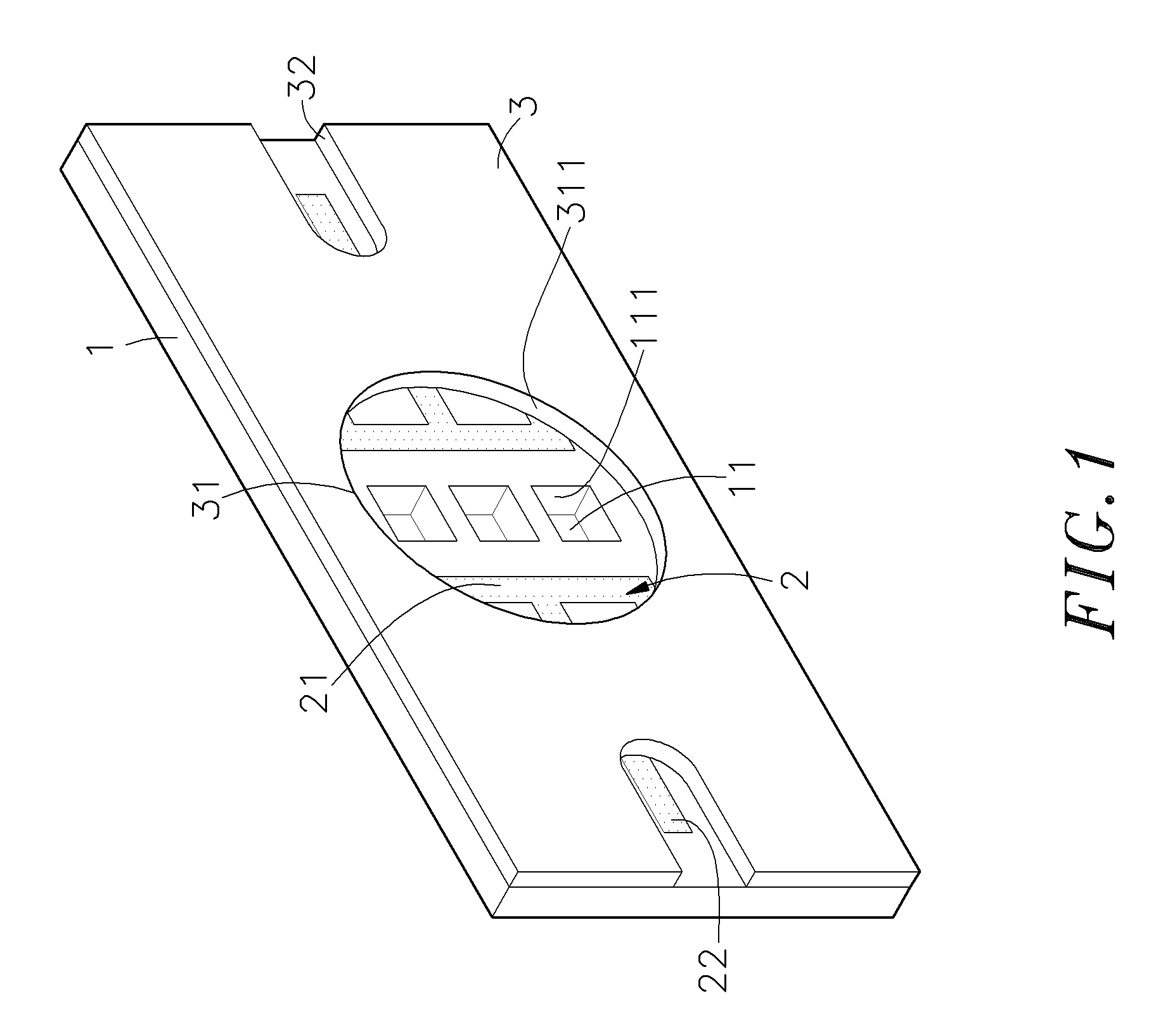
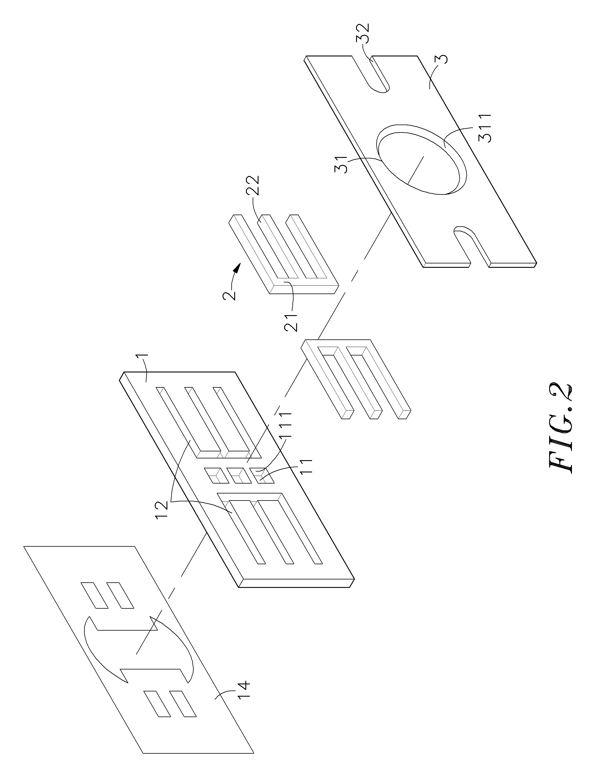
[0025]Referring to FIGS. 1, 2, 3, 4 and 5, a packaging structure of the present invention is shown comprised of a metal plate 1, complex insulators 2 and a cover plate 3.

[0026]The metal plate 1 comprises at least one containing slot 11 in the form of concave cone at the center surface, two isolating slots 12 established in opposite directions on the outer sides of the containing slot 11, two soldering portions 13 at the bottom side between the containing slot 11 and the isolating slots 12, and an anti-soldering layer 14 formed on the external edge of the soldering portions 13. In addition, the containing slot 11 has a light-conducting surface 111 at vertical or inclination angle on inner wall thereof.

[0027]The insulators 2 are set in the size that fits with the isolating slots 12. Each of the insulators 2 comprises a base 21, and extended portions 22 arranged at an interval extended from one side of the base 21.

[0028]The cover plate 3 comprises a circular hollow slot 31 at the cente...


PUM


Abstract

The present invention relates to a packaging structure for high-power light emitting diode (LED) chip, comprising a metal plate, insulators and a cover plate. The metal plate comprises a containing slot and isolating slots formed on the surface by working, and the insulators can be embedded in the isolating slot. After forming a hollow slot and notches on the surface of the cover plate by working, the cover plate is combined with the metal plate and insulators and at the same time, the hollow slot and the notches are corresponding to the containing slot and the isolating slots on the metal plate to form a hollowness state, followed by application of surface treatment to form soldering portions and an anti-soldering layer at the bottom of the metal plate. Then the metal plate is cut on both sides along free ends of the insulators so as to generate electrode contacts with positive and negative electrodes, and the surface mount technology (SMT) can be adopted for assembly of the packaging structure of high-power LED chip so as to simplify manufacturing processes, facilitate mass production and achieve separation of electricity from heat, etc.

Description

BACKGROUND OF THE INVENTION[0001]1. Field of the Invention[0002]The present invention relates to a packaging structure for high-power LED chip, especially to a packaging structure for high-power LED chip that can achieve such functions as simplifying manufacturing processes, facilitating mass production and isolating electricity from heat, etc., which is formed by embedding the insulators in the metal plate, combining the cover plate with the metal plate and the insulators and cutting the metal plate on both sides along the free ends of the insulators to form electrode contacts.[0003]2. Description of Related Art[0004]With regard to the structure of the chip on board (COB) for the conventional chips, take the packaging of LED chip as an example and refer to FIG. 10. A chip A is mounted in a flex arc B1 of an insulator B and a wire A1 connected and extended from the chip A is connected with a positive electrode pin C and a negative electrode pin D installed in the insulator B respect...

Claims


Application Information

Patent Timeline
IPC IPC(8): H01L33/00
CPCH01L25/0753H01L33/486H01L33/62H01L33/642H01L2224/48247H01L2224/48091H01L2924/00014H01L2224/48257H01L2924/181H01L2924/00012
Inventor CHANG, CHUNG-CHIYU, HAO-JAN
Owner BRILLIANT TECH
Why Eureka
Try Eureka