Method of fabricating transparent conductive film

a technology of transparent conductive film and conductive film, which is applied in the direction of vacuum evaporation coating, coating, sputtering coating, etc., can solve the problems of glass substrate being too brittle to extra work, increasing the weight of the touch panel, and being more easily cut but not maintained at a high temperature. , to achieve the effect of improving the specific speed, improving the physical and electrical properties, and slowing down the specific speed

Inactive Publication Date: 2010-04-29
APPLIED VACUUM COATING TECH
View PDF15 Cites 0 Cited by
  • Summary
  • Abstract
  • Description
  • Claims
  • Application Information

AI Technical Summary

Benefits of technology

[0017]In one embodiment of the present invention, the higher the working temperature is, the higher the specific speed is, while the lower the working temperature is, the slower the specific speed is.
[0018]In the present invention, when the hard plastic substrate is passed through the reactive chamber, the hard plastic substrate is instantly heated. Such instantly high temperature environment will get the better physical and electrical properties of the transparent conductive film. In addition, the period of time that the hard plastic substrate is passed through the reactive chamber may also be adjusted in response to different temperatures of the reactive chamber to prevent the plastic substrate from deformation. As such, the present invention provides a method of fabricating transparent conductive film on a hard plastic substrate.

Problems solved by technology

However, the glass substrate is too brittle to extra work and also may increase weight of the touch panel 100.
A hard plastic substrate such as a polycarbonate substrate has lighter weight and may be more easily cut but cannot maintain at a high temperature under a sputtering process.
As a result, the laminating process which transfers the PET film with transparent conductive film onto the PC increases manufacturing costs and decreases yield due to the laminating process.
Accordingly, not only do the manufacturing costs add up but also the thickness of the touch panel 100 increases, resulting in low transmittance of the visible light.

Method used


Image

  • Method of fabricating transparent conductive film
  • Method of fabricating transparent conductive film
  • Method of fabricating transparent conductive film

Examples


Embodiment Construction

[0026]A plastic substrate is only capable of bearing a low range of working temperature so transparent conductive film cannot be coated on a plastic substrate directly using a conventional sputtering process. Thus, the application aspect of a plastic substrate is greatly limited. Based on the above reason, the present invention provides a method of fabricating transparent conductive film, wherein the transparent conductive film is directly formed on a hard plastic substrate and has good conductivity. In addition, the hard plastic substrate adopted in the method of the present invention will not be deformed or damaged due to the heat.

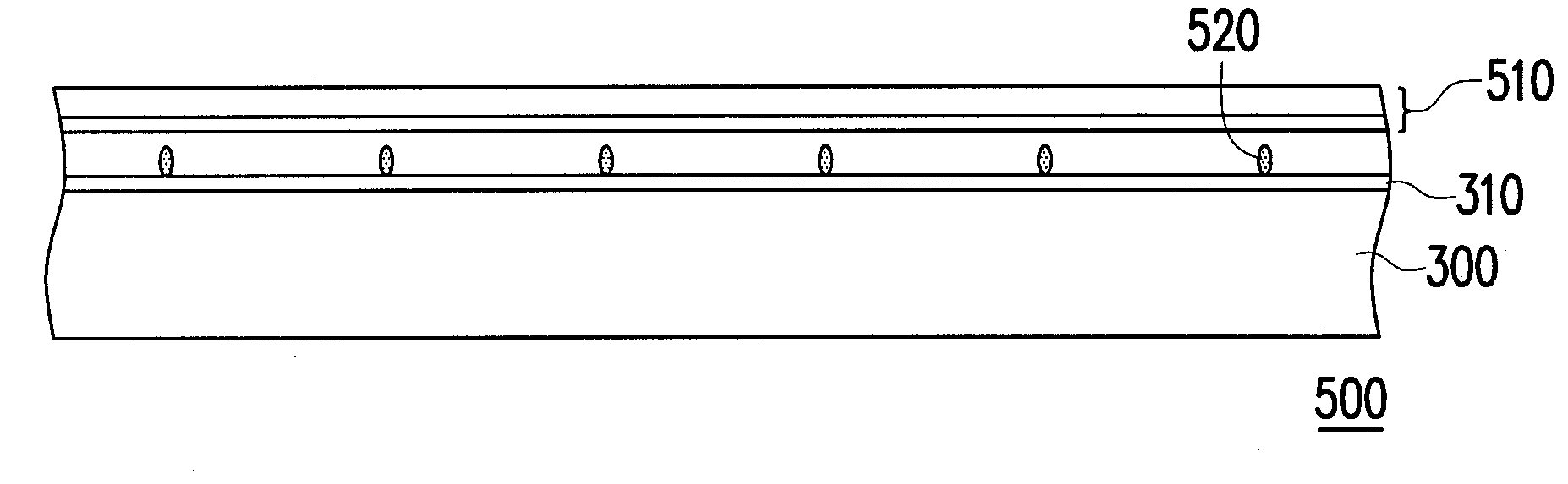
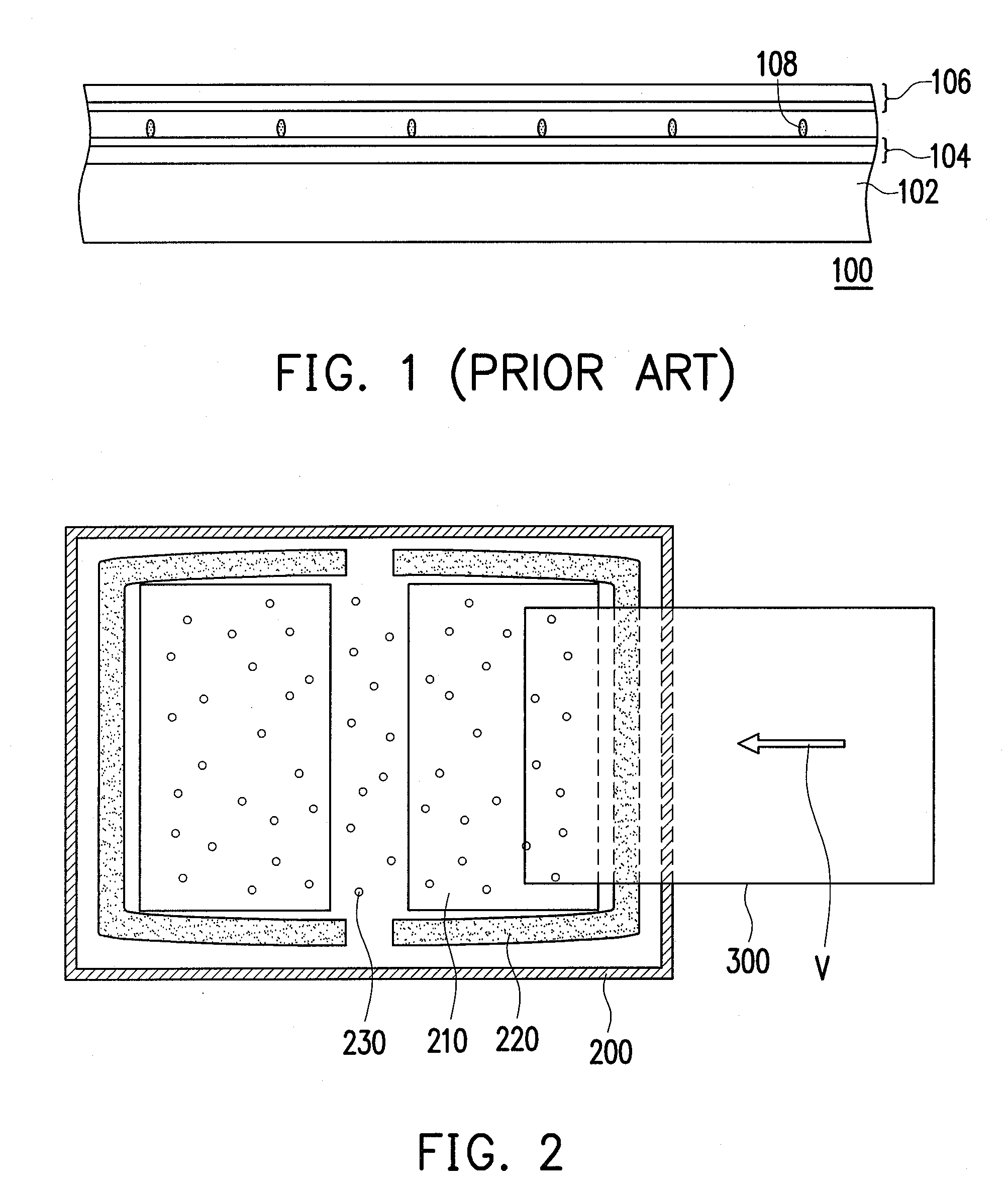
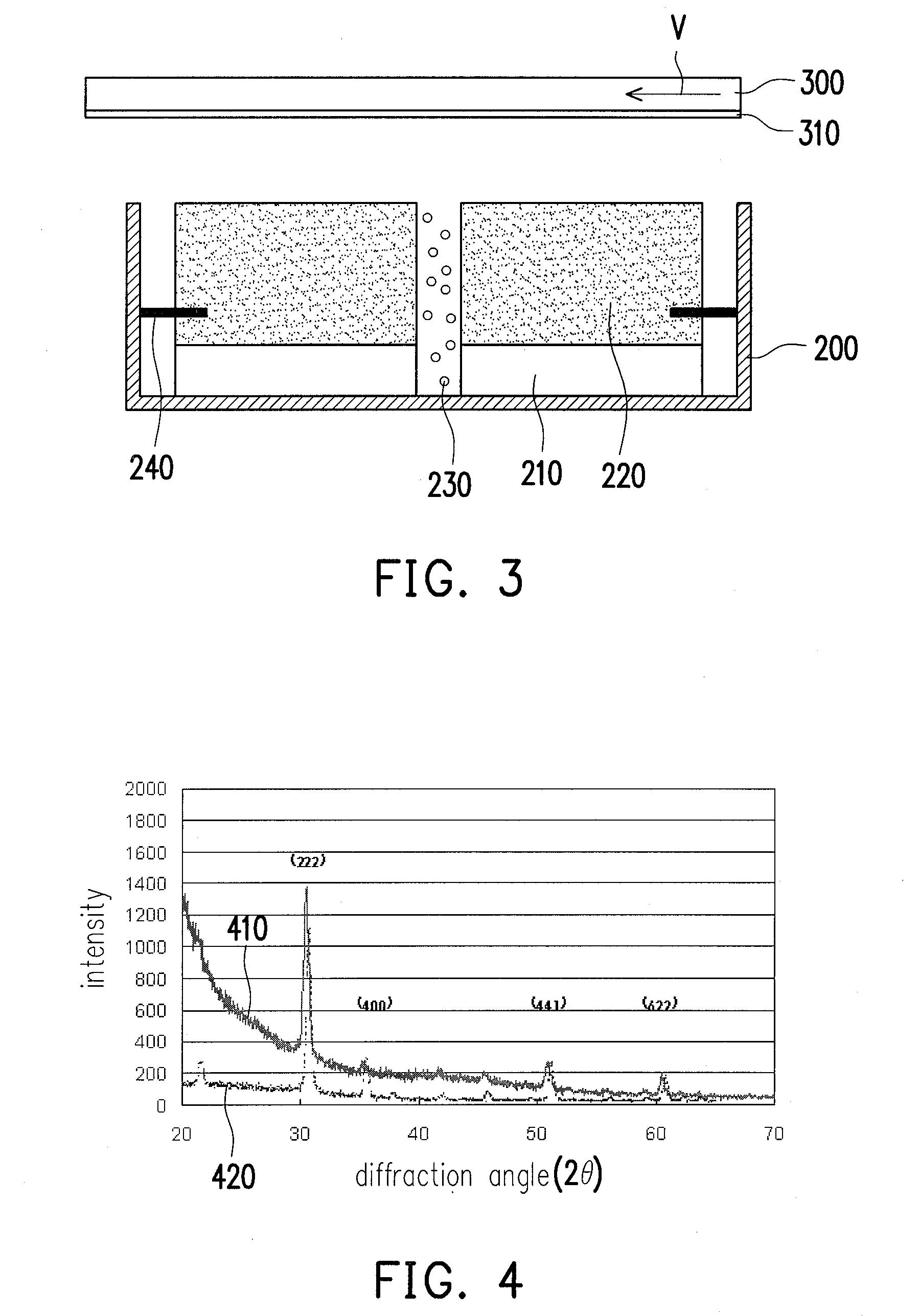
[0027]FIG. 2 is a top view illustrating the flow of fabricating transparent conductive film in one embodiment of the present invention. FIG. 3 is a lateral view illustrating the flow of fabricating transparent conductive film in one embodiment of the present invention. Referring to both FIG. 2 and FIG. 3, the method of fabricating transparent conductive ...


PUM

PropertyMeasurementUnit
standby temperatureaaaaaaaaaa
temperatureaaaaaaaaaa

Abstract

A method of fabricating transparent conductive film including the following steps is provided. First, a reactive chamber having at least a target and at least a heating device is provided. Subsequentially, a plasma is generated in the reactive chamber, wherein the plasma is located above the target. Next, the plasma is heated by the heating device from a standby temperature to a working temperature. Simultaneously, a hard plastic substrate is passed above the plasma at a specific speed, wherein the particles of the target are bombarded by the plasma so as to form transparent conductive film on the hard plastic substrate.

Description

BACKGROUND OF THE INVENTION[0001]1. Field of the Invention[0002]The present invention relates to a method of fabricating conductive film. More particularly, the present invention relates to a method of fabricating transparent conductive film.[0003]2. Description of Related Art[0004]With the gradual development in the semiconductor technology, transparent conductive film has been widely applied in electronic devices of various fields. For example, transparent conductive film is applied in the fields such as the pixel electrodes and the opposite electrodes used to maintain a display voltage in a liquid crystal display and the sensor electrodes in a touch panel. The components of transparent film are mostly metal oxide layers such as Indium Tin Oxide (ITO) or Indium Zinc Oxide (IZO), which have the characteristics of both light transmittance and conductivity at a certain optical thickness.[0005]A touch panel is illustrated below as an example. FIG. 1 is a schematic view of a touch pane...

Claims


Application Information

Patent Timeline
Patent Type & Authority Applications(United States)
IPC IPC(8): C23C14/34
CPCC23C14/025C23C14/34C23C14/086
Inventor WENG, CHIEN-MINCHU, TZU-WENHUANG, CHIAO-NINGLEE, I-WENCHOU, SHIH-LIANG
Owner APPLIED VACUUM COATING TECH
Why Eureka
Try Eureka