Semiconductor device using graphene and method of manufacturing the same

a graphene and semiconductor technology, applied in semiconductor devices, digital storage, instruments, etc., can solve the problems of inability to produce, disadvantageous electric power consumption, poor on/off ratio, etc., and achieve low electric power consumption, high speed operation, and reduce material cost

Active Publication Date: 2010-04-29
NEC CORP
View PDF3 Cites 123 Cited by
  • Summary
  • Abstract
  • Description
  • Claims
  • Application Information

AI Technical Summary

Benefits of technology

[0022]According to the present invention, it is possible to provide a semiconductor device which is made compact on a two-dimensional plane and provided with high speed operation and low electric power consumption by using graphene having a controlled edge structure with a width of 20 nm or less, with which the quantum size effect is significant, and also to provide a method of manufacturing the same.
[0023]Furthermore, according to the present invention, it is possible to provide a semiconductor device which can reduce material cost by uniformly using graphene for all of components such as channels, electrodes, and interconnections of the semiconductor device and can reduce manufacturing cost by avoiding using materials other than graphene and simplifying manufacturing steps, and also to provide a method of manufacturing the same.

Problems solved by technology

First, the field-effect transistors have a very poor on / off ratio of about 10 to about 102 and do not establish an off state in practical use. Therefore, the electric power consumption is disadvantageously huge. This is attributable to the fact that a metal graphene is used as a channel. The reason is because a metal can increase and decrease the carrier density of the channel to some extent with an electric field of a gate electrode but cannot make the carrier density completely zero.
Second, the field-effect transistors have a problem that p-type and n-type conduction channels cannot be produced separately because they demonstrate ambipolar conduction. Therefore, a low-power-consumption inverter or the like cannot be formed by combining p-type and n-type transistors in a complementary manner. This is attributable to the fact that conduction electrons are induced in the channel in a case of a negative gate voltage while positive holes are induced in the channel in a case of a positive gate voltage. The reason is because a graphene demonstrates ambipolar conduction in the first place and has the same number of positive holes and electrons therein under no electric field.

Method used


Image

  • Semiconductor device using graphene and method of manufacturing the same
  • Semiconductor device using graphene and method of manufacturing the same
  • Semiconductor device using graphene and method of manufacturing the same

Examples


example 1

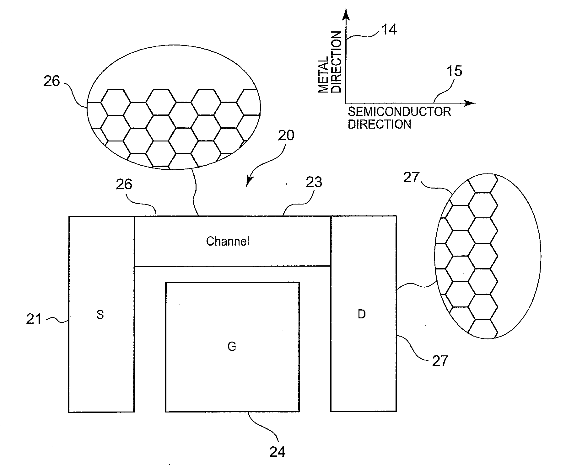
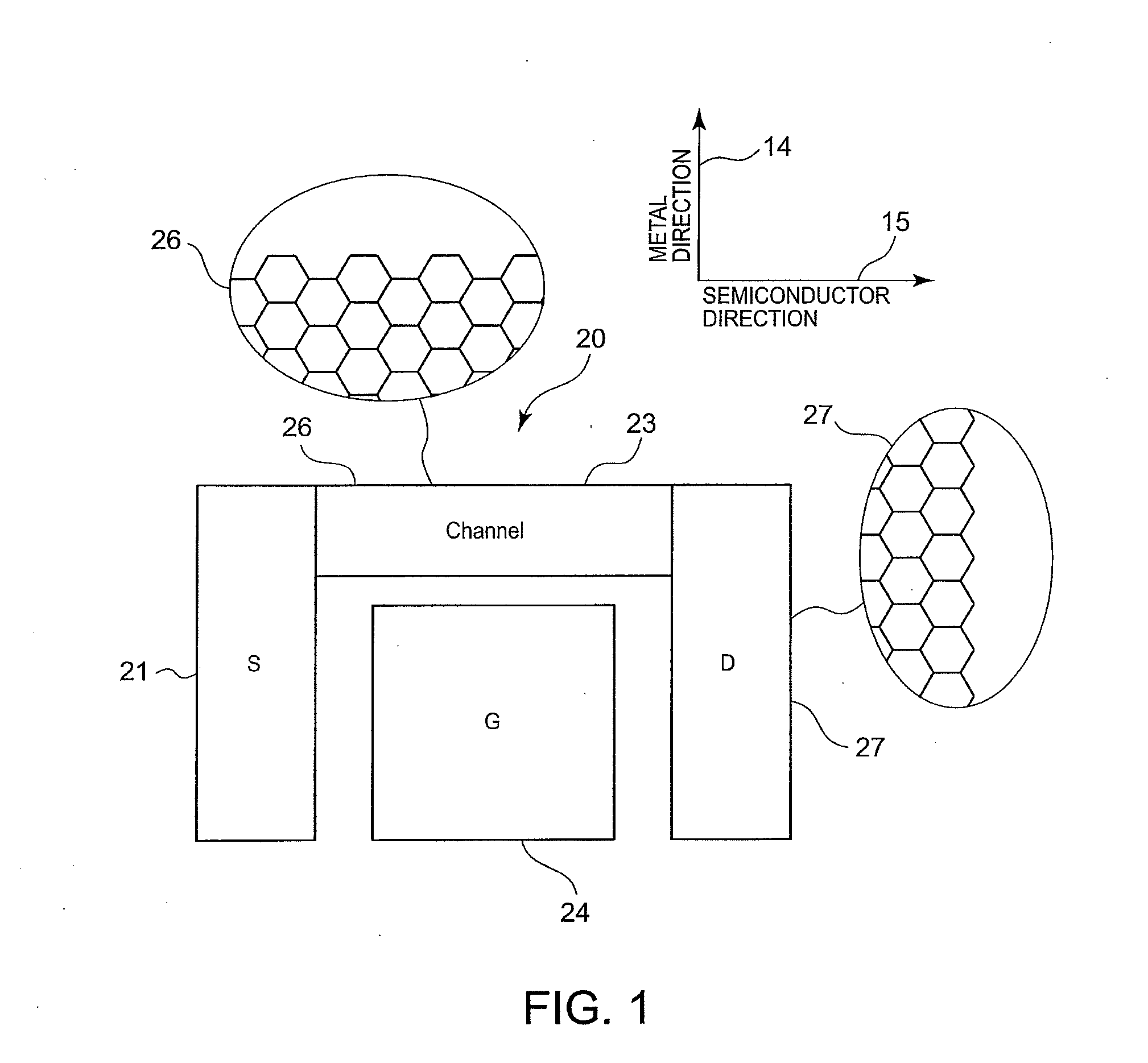
[0084]FIG. 6 is a diagram showing a full-graphene double-gate field-effect transistor produced by the manufacturing method shown in FIGS. 5A to 5D.

[0085]Referring to FIG. 6, a full-graphene double-gate field-effect transistor 20 has a structure including a source electrode 21 formed of metal graphene integrally with interconnections, a drain electrode 22 formed of metal graphene integrally with interconnections, a channel 23 formed so as to connect the source electrode 21 and the drain electrode 22 to each other, and two gate electrodes 24 and 25 opposed to each other so as to interpose the channel 23 therebetween. The advantages of this structure include the following two aspects.

[0086]One aspect is excellent gate controllability and readiness to establish an off state because electric fields from the two gate electrodes 24 and 25 can be applied symmetrically to the channel.

[0087]The other aspect is that, when the two gate electrodes 24 and 25 are designed asymmetrically in size, i...

example 2

[0088]FIGS. 7A to 7C are diagrams showing complementary inverters 30a, 30b, and 30c of a full-graphene device produced by the same manufacturing method as shown in FIGS. 5A to 5D. FIG. 7A shows an inverter in which p-type and n-type channels are controlled by two independent gate electrodes. FIG. 7B shows an inverter in which p-type and n-type channels are positioned on the same line and controlled by one gate electrode. FIG. 7C shows an inverter in which p-type and n-type channels are positioned in parallel to each other and controlled by one gate electrode.

[0089]Referring to the complementary inverter 30a in FIG. 7A, a p-type channel 31 and an n-type channel 32 are formed of semiconductor graphene, and electrodes such as gate electrodes 33, which also serve as interconnections, are formed of metal graphene. The reference numeral 34 denotes an output voltage Vout, the reference numeral 35 an input voltage Vin, the reference numeral 37 a power source voltage VDD, and the reference n...

example 3

[0098]FIGS. 8A to 8C are diagrams showing NOR gates 40a, 40b, and 40c of complementary inverters produced by the manufacturing method shown in FIGS. 5A to 5D.

[0099]In FIGS. 8A to 8C, the number of gate electrodes is two in the NOR gate 40a of FIG. 8A, four in the NOR gate 40b of FIG. 8B, and three in the NOR gate 40c of FIG. 8C. The reference numeral 41 denotes three equivalent directions of a semiconductor graphene, and the reference numeral 42 denotes three equivalent directions of a metal graphene. Those directions are common to FIGS. 8A, 8B, and 8C.

[0100]The NOR gate 40a shown in FIG. 8A has the smallest number of gate electrodes. Outputs (Vout) 34 should be drawn out of the plane through vias 38. The reference numerals 31a and 31b denote first and second p-type channels of semiconductor graphene, respectively, and the reference numerals 32a and 32b denote first and second n-type channels of semiconductor graphene, respectively. The reference numerals 33a and 33b denote first an...


PUM

PropertyMeasurementUnit
widthaaaaaaaaaa
ionization energyaaaaaaaaaa

Abstract

A semiconductor graphene is used for a channel layer, and a metal graphene is used for electrode layers for a source, a drain, and a gate which serve as interconnections as well. An oxide is used for a gate insulating layer. The channel layer and the electrode layers are located on the same plane.

Description

TECHNICAL FIELD[0001]The present invention relates to a semiconductor device and a method of manufacturing the same. More particularly, the present invention relates to a field-effect transistor including a p-type channel or an n-type channel operable at an ultrahigh speed with low electric power consumption in which all component elements such as a channel, electrodes for a gate, a source, and a drain, and interconnections are formed of graphene, a semiconductor device such as a logic circuit or a memory cell circuit which combines such field-effect transistors, and a method of manufacturing such a semiconductor device.BACKGROUND ART[0002]The current information-oriented society is supported by semiconductor devices represented by CMOS (complementary metal oxide semiconductors) based on silicon. The silicon semiconductor industry has heretofore achieved miniaturization with both of high integration and high performance by continuously decreasing applicable ranges of microfabricatio...

Claims


Application Information

Patent Timeline
Patent Type & Authority Applications(United States)
IPC IPC(8): H01L29/167H01L21/04
CPCB82Y10/00H01L29/78684H01L21/8213H01L21/8221H01L21/823807H01L21/823828H01L27/0207H01L27/0688H01L27/088H01L27/092H01L27/11H01L27/1104H01L29/0665H01L29/0673H01L29/16H01L29/1606H01L29/7781G11C11/412Y10S977/755H10B10/00H10B10/12
Inventor HIURA, HIDEFUMINIHEI, FUMIYUKITADA, TETSUYAKANAYAMA, TOSHIHIKO
Owner NEC CORP
Why Eureka
Try Eureka