Switching element and manufacturing method thereof

a technology of switching element and manufacturing method, which is applied in the field of switching element, can solve the problems of difficult effective suppression and difficult effective control of the switching phenomenon of the active layer by the gate bias voltage, and achieve excellent and stable transistor characteristics, improve interaction

Active Publication Date: 2010-04-29
NEC CORP
View PDF3 Cites 7 Cited by
  • Summary
  • Abstract
  • Description
  • Claims
  • Application Information

AI Technical Summary

Benefits of technology

[0015]Therefore, an object of the present invention is to provide a switching element which enhances the interaction between CNTs and the gate dielectric film and exhibits excellent and stable transistor characteristics.
[0017]After keen examination for solving the above-mentioned problems, the present inventors have found that the interaction between the surface of the gate dielectric film and CNTs can be improved by forming the gate dielectric film from non-conjugated polymer containing an aromatic ring in the side chain as described above. Thereby, a switching element which exhibits excellent and stable transistor characteristics can be obtained with a low-temperature, convenient and inexpensive process.
[0019]In the above-mentioned switching element, in one aspect, it is preferable that the gate dielectric film is formed of a single-layer film. In another aspect, it is preferred that the gate dielectric film has a first gate dielectric film layer which is in contact with the active layer and a second gate dielectric film layer which is not in contact with the active layer and the non-conjugated polymer is contained in the first gate dielectric film layer. As described above, the gate dielectric film may have a two-layered structure. In the case where the two-layered structure is used, the interaction between the CNTs and the gate dielectric film can be improved, when the above-mentioned non-conjugated polymer is contained in the layer in contact with the active layer (first gate dielectric film layer).
[0020]In the above-mentioned switching element, in one aspect, it is preferable that the non-conjugated polymer is polymer including at least one type of repeated units A having an aromatic ring in the side chain. In another aspect, it is preferable that the non-conjugated polymer is a copolymer including at least one type of repeated units A having the aromatic ring in the side chain and at least one type of repeated units B having no aromatic ring in the side chain, and the repeated units A are contained five times or more as much as the repeated units B in mole ratio. When the polymer including only the repeated units A is used, the density of the aromatic ring increases and the interaction between the gate dielectric film and the active layer can be improved. On the other hand, if the repeated units B having no aromatic rings in the side chain are introduced in addition to the repeated units A having an aromatic ring in the side chain, the non-conjugated polymer can be prevented from becoming rigid due to the existence of the aromatic ring. When the content of the repeated units A is less than five times of the content of the repeated units B in mole ratio, the density of the aromatic group becomes insufficient and the interaction between the gate dielectric film and the CNTs also tends to become insufficient.
[0021]In the above-mentioned switching element, it is preferable that the non-conjugated polymer includes substituted polyethylene skeletons represented by the below-mentioned structural formula as the repeated units:In the formula, X represents a linking group or a single bond, Ar represents an aromatic group having the aromatic ring and n represents a positive integer. The non-conjugated polymer having such a substituted polyethylene skeleton is easy to be subjected to resin treatment and inexpensive. Accordingly, non-conjugated polymer with a desired structure can be obtained at low costs.
[0029]According to the present invention, a switching element is provided which improves the interaction between CNTs and the gate dielectric film and exhibits excellent and stable transistor characteristics.

Problems solved by technology

When the thickness is smaller than 0.01 μm, it is difficult to effectively suppress a leak current, and when the thickness is larger than 1.0 μm, it is difficult to effectively control switching phenomenon of the active layer by the gate bias voltage.

Method used


Image

  • Switching element and manufacturing method thereof
  • Switching element and manufacturing method thereof
  • Switching element and manufacturing method thereof

Examples


first embodiment

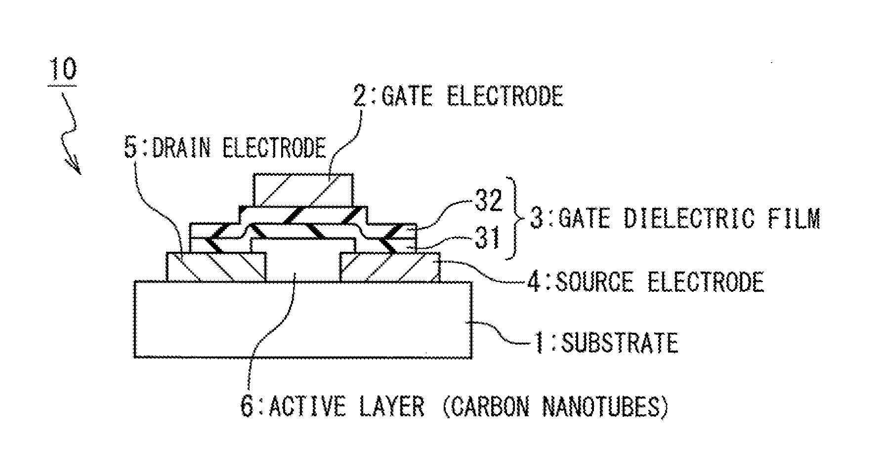
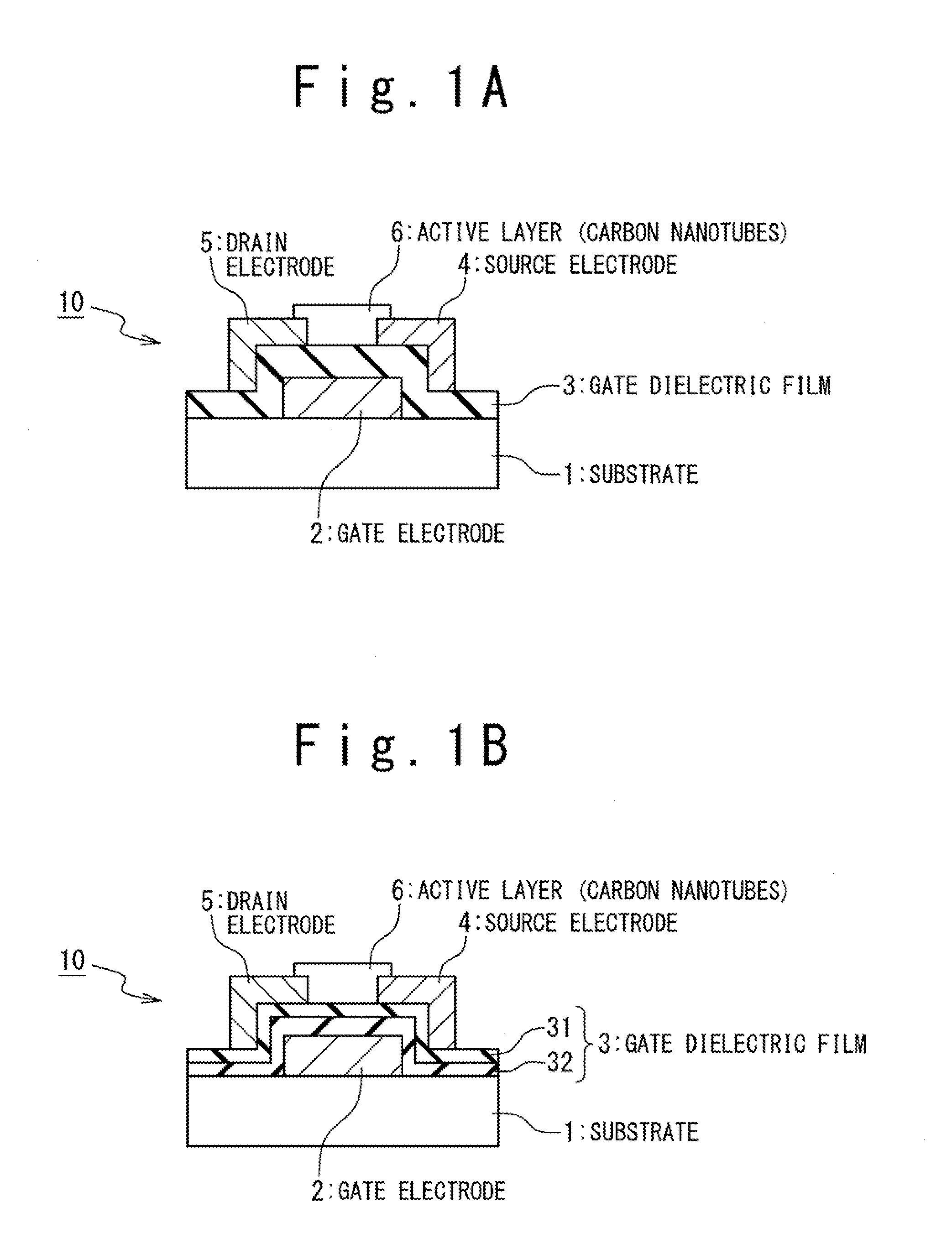
[0034]The configuration of a switching element 10 in a first embodiment of the present invention will be described referring to the Drawings.

[0035]FIG. 1A is a schematic sectional view showing the configuration of the switching element 10 according to the present invention. As shown in FIG. 1A, the switching element 10 includes: a supporting substrate 1; a gate electrode 2 formed on the supporting substrate 1; a gate dielectric film 3 provided on the supporting substrate 1 so as to cover the gate electrode 2; source and drain electrodes 4 and 5 which are provided on the gate dielectric film 3 at a distance therebetween corresponding to the channel length; and an active layer 6 provided in contact with all of the gate dielectric film 3, the source electrode 4 and the drain electrode 5. As described above, the switching element 10 in the present embodiment is a so-called bottom-contact type thin film transistor.

[0036]The material of the supporting substrate 1 is not specifically limit...

second embodiment

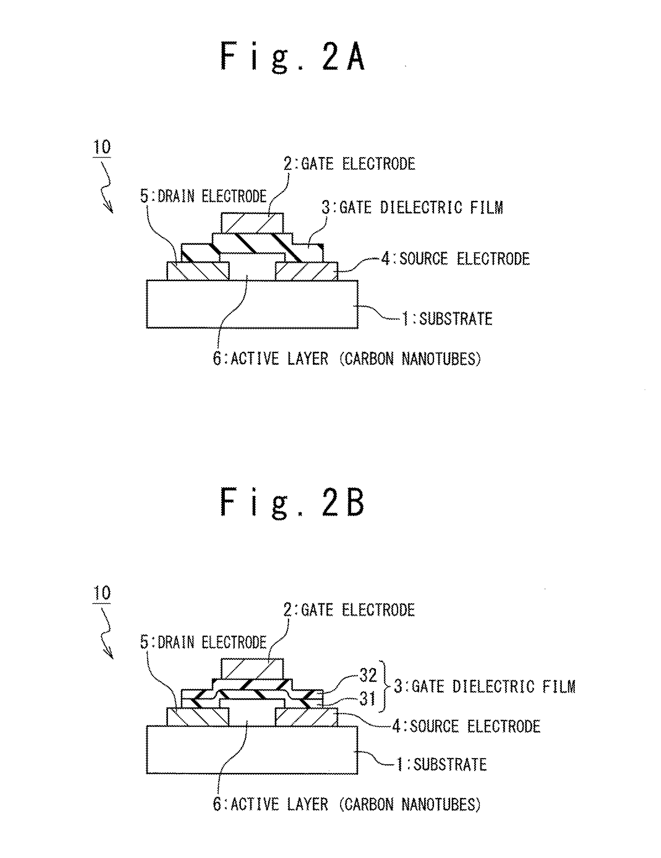
[0065]Subsequently, a description is given of a second embodiment of the present invention. FIG. 2A is a schematic sectional view of a switching element 10 of this embodiment. As shown in FIG. 2A, the switching element 10 of this embodiment includes: a supporting substrate 1; source and drain electrodes 4 and 5 which are disposed on the supporting substrate 1 with a distance therebetween corresponding to the channel length; an active layer 6 formed so as to be in contact with these electrodes, a gate dielectric film 3 formed on the source electrode 4, the drain electrode 5 and the active layer 6 and the gate electrode 2 formed on the gate dielectric film 3. That is, the switching element 10 according to the present embodiment has a top-contact structure in which the gate electrode 2 exists on an opposite side to the supporting substrate 1 across the active layer 6. Since materials for the supporting substrate 1, the source electrode 4, the drain electrode 5, the active layer 6, the ...

embodiment 1

[0070]A description is given of a method of manufacturing the switching elements 10 of Embodiment 1. The structure of the switching elements 10 of Embodiment 1 is the same as that shown in FIG. 1A. First, a polyethylene naphthalate substrate having a thickness of 0.5 mm was prepared as the supporting substrate 1 and an aluminum film of 100 nm was formed as the gate electrode 2 on the supporting substrate 1 by using a shadow mask according to the sputtering method. Next, a xylene solution of polystyrene (non-conjugated polymer having a aromatic group in the side chain) was applied as the gate dielectric film 3 by a spin coat method and dried at 120° C. to form a film having a thickness of 100 nm. Gold was deposited thereon as the source and drain electrodes 4 and 5 by a vacuum deposition method through a shadow mask so that the source and drain electrodes 4 and 5 have a thickness of 60 nm. In this electrode structure thus formed, the channel width and length were 200 μm and 50 μm, re...


PUM

PropertyMeasurementUnit
thicknessaaaaaaaaaa
thicknessaaaaaaaaaa
thicknessaaaaaaaaaa

Abstract

Disclosed is a switching element provided with a gate dielectric film and an active layer disposed in contact with the gate dielectric film. The active layer includes carbon nanotubes, and the gate dielectric film includes non-conjugated polymer containing an aromatic ring in a side chain.

Description

TECHNICAL FIELD[0001]This application is based on Japanese Patent Application filed on Mar. 2, 2007 (Application Number: Japanese Patent Application No. 2007-053512) and claims the benefit of priority to the Japanese Patent Application, and the entire disclosure of the Japanese Patent Application is incorporated herein by reference.[0002]The present invention relates to a switching element having an active layer using carbon nanotubes (hereinafter also referred to as CNTs).BACKGROUND ART[0003]Thin film transistors (TFTs) have been widely used as pixel switching elements in display devices such as liquid crystal displays and EL displays. In recent years, a pixel array driver circuit using TFTs has been increasingly formed on the same substrate. Conventionally, such TFTs have been formed on a glass substrate using amorphous or polycrystalline silicon.[0004]A CVD apparatus used for forming such a TFT using silicon is very expensive and an increase in the area of the display device usin...

Claims


Application Information

Patent Timeline
Patent Type & Authority Applications(United States)
IPC IPC(8): H01L29/16H01L21/04
CPCB82Y10/00H01L29/0665H01L29/0669H01L29/0673H01L51/004H01L51/0048Y10S977/708H01L51/0529H01L51/0541H01L51/0545H01L51/0558H01L51/0566Y10S977/742H01L51/052H10K85/141H10K85/221H10K10/471H10K10/474H10K10/464H10K10/484H10K10/488H10K10/466
Inventor TOGUCHI, SATORUISHIDA, MASAHIKOENDOH, HIROYUKI
Owner NEC CORP
Why Eureka
Try Eureka