Method for producing group III nitride semiconductor and template substrate

a technology of nitride semiconductor and template substrate, which is applied in the direction of semiconductor devices, basic electric elements, electrical apparatus, etc., can solve the problems of deterioration of device performance, method failure to mass-produce such a gan substrate, and inability to increase the size of the substrate, etc., to achieve excellent crystallinity and surface flatness, effective etch

Active Publication Date: 2010-04-29
TOYODA GOSEI CO LTD
View PDF24 Cites 22 Cited by
  • Summary
  • Abstract
  • Description
  • Claims
  • Application Information

AI Technical Summary

Benefits of technology

[0059]When a stripe-pattern groove whose longitudinal side surfaces are a-plane of sapphire is provided, there can be produced a Group III nitride semiconductor whose main surface is a non-polar plane or a semi-polar plane and which exhibits excellent crystallinity and surface flatness.
[0060]The method of the present invention may employ dry etching. The growth substrate can be effectively etched by means of ICP etching.
[0061]In the template substrate according to any of the third to sixth aspects of the present invention, the Group III nitride semiconductor layer exhibits excellent crystallinity and surface flatness. When a semiconductor device is produced by stacking a Group III nitride semiconductor layer on the template substrate, the resultant semiconductor device is not affected by a piezoelectric field.

Problems solved by technology

However, due to strain in the crystal structure of the Group III nitride semiconductor, a piezoelectric field is generated in a c-axis direction of the semiconductor, which may cause deterioration of device performance.
However, when an m-plane or a-plane GaN substrate is produced through a conventional method, the size of the substrate cannot be increased, since the substrate size depends on the thickness of a GaN layer.
In addition, the conventional method fails to mass-produce such a GaN substrate.
The method disclosed in Japanese Patent Application Laid-Open (kokai) No. 2006-36561 encounters difficulty in selectively forming a mask or a buffer layer, and in growing, with high reproducibility, a Group III nitride semiconductor exhibiting good crystallinity and having an a-plane or m-plane main surface.

Method used


Image

  • Method for producing group III nitride semiconductor and template substrate
  • Method for producing group III nitride semiconductor and template substrate
  • Method for producing group III nitride semiconductor and template substrate

Examples


embodiment 1

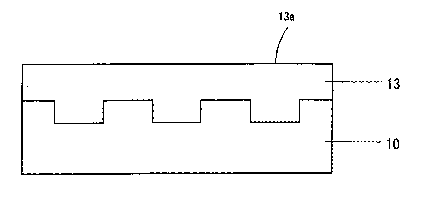
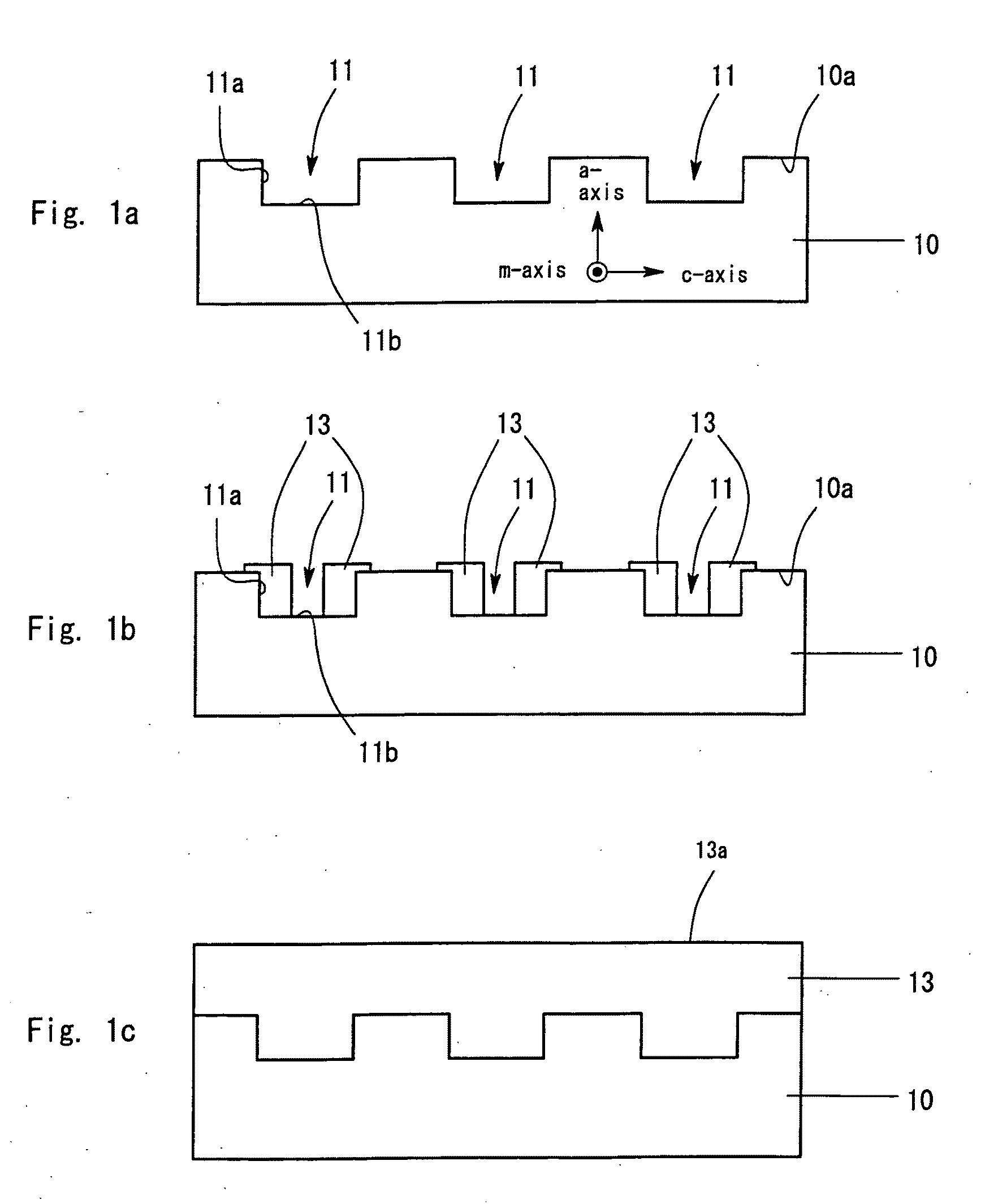
[0073]Embodiment 1 corresponds to a method for producing a GaN template substrate having an m-plane main surface. Steps of the production method will now be described with reference to FIGS. 1A to 1C.

(Groove Formation Step)

[0074]Firstly, a surface 10a of a sapphire substrate 10 having an a-plane main surface (corresponding to the growth substrate of the present invention) is subjected to ICP etching by use of a mask, to thereby form stripe-pattern grooves 11 whose longitudinal direction is parallel to the m-axis direction of the sapphire substrate 10 (FIG. 1A). The cross section of each groove 11 parallel to the c-axis assumes a rectangular form. C-plane surfaces of the sapphire substrate are exposed at the side surfaces 11a of each groove 11, and an a-plane surface of the sapphire substrate is exposed at the bottom surface 11b of the groove 11.

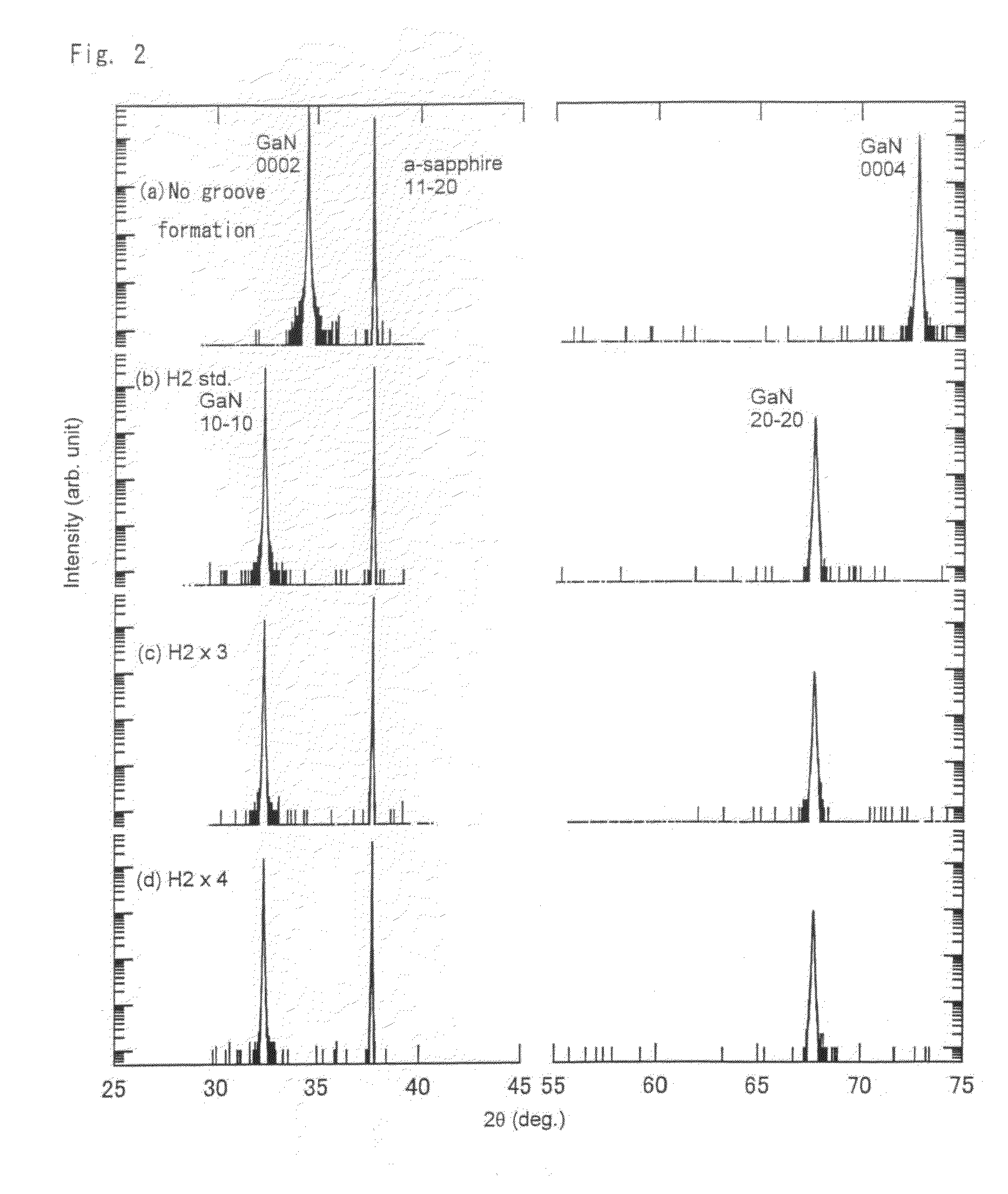
[0075]In general, after formation of the grooves 11, the sapphire substrate 10 is heated to 1,000° C. or higher for restoring damage to the ...

embodiment 2

[0093]Similar to the case of Embodiment 1, Embodiment 2 corresponds to a method for producing a GaN template substrate having an m-plane main surface. Steps of the production method will next be described with reference to FIGS. 5A to 5D.

(Groove Formation Step)

[0094]Firstly, a surface 10a of a sapphire substrate 10 having an a-plane main surface (corresponding to the growth substrate of the present invention) is subjected to ICP etching by use of a mask, to thereby form stripe-pattern grooves 11 whose longitudinal direction is parallel to the m-axis direction of the sapphire substrate 10 (FIG. 5A). The cross section of each groove 11 parallel to the c-axis assumes a rectangular form. C-plane surfaces of the sapphire substrate are exposed at the side surfaces 11a of each groove 11, and an a-plane surface of the sapphire substrate is exposed at the bottom surface 11b of the groove 11.

(Buffer Film Formation Step)

[0095]Subsequently, the sapphire substrate 10 having the thus-formed groov...


PUM

PropertyMeasurementUnit
depthaaaaaaaaaa
depthaaaaaaaaaa
widthaaaaaaaaaa

Abstract

The present invention provides a method for producing a Group III nitride semiconductor. The method includes forming a groove in a surface of a growth substrate through etching; forming a buffer film on the groove-formed surface of the growth substrate through sputtering; heating, in an atmosphere containing hydrogen and ammonia, the substrate to a temperature at which a Group III nitride semiconductor of interest is grown; and epitaxially growing the Group III nitride semiconductor on side surfaces of the groove at the growth temperature. The thickness of the buffer film or the growth temperature is regulated so that the Group III nitride semiconductor is grown primarily on the side surfaces of the groove in a direction parallel to the main surface of the growth substrate. The thickness of the buffer film is regulated to be smaller than that of a buffer film which is employed for epitaxially growing the Group III nitride semiconductor on a planar growth substrate uniformly in a direction perpendicular to the growth substrate. The growth temperature is regulated to be lower than a temperature at which the Group III nitride semiconductor is epitaxially grown on a planar growth substrate uniformly in a direction perpendicular to the growth substrate. The growth temperature is preferably 1,020 to 1,100° C. The buffer film employed is an AlN film having a thickness of 150 Å or less.

Description

BACKGROUND OF THE INVENTION[0001]1. Field of the Invention[0002]The present invention relates to a method for producing a Group III nitride semiconductor product whose main surface is a non-polar plane (e.g., m-plane or a-plane) or a semi-polar plane (e.g., r-plane). The present invention also relates to a template substrate including a growth substrate and a Group III nitride semiconductor whose main surface is a non-polar plane or a semi-polar plane, the Group III nitride semiconductor being formed on the growth substrate.[0003]2. Background Art[0004]Hitherto, Group III nitride semiconductor device have been produced by stacking a Group III nitride semiconductor on a growth substrate (e.g., a sapphire substrate) in a c-axis direction. However, due to strain in the crystal structure of the Group III nitride semiconductor, a piezoelectric field is generated in a c-axis direction of the semiconductor, which may cause deterioration of device performance. When, for example, a light-emi...

Claims


Application Information

Patent Timeline
Patent Type & Authority Applications(United States)
IPC IPC(8): H01L29/20H01L21/203H01L29/06
CPCH01L21/0237H01L21/0242H01L21/02433H01L21/02458H01L29/2003H01L21/0262H01L21/02636H01L21/02639H01L21/02647H01L21/0254H01L29/045
Inventor NAKADA, NAOYUKIOKUNO, KOJIUSHIDA, YASUHISA
Owner TOYODA GOSEI CO LTD
Why Eureka
Try Eureka