Flexible nanoimprint mold, method for fabricating the same, and mold usage on planar and curved substrate

a nanoimprint and mold technology, applied in the field of nanoimprint technology, can solve the problems of limiting the application, difficult to extend current nanoimprint lithography to a curved substrate, stiff molds cannot provide conformal contact with non-planar surfaces, etc., and achieve the effect of ultra-fine resolution pattern transfer

Active Publication Date: 2010-05-06
NANJING UNIV
View PDF6 Cites 57 Cited by
  • Summary
  • Abstract
  • Description
  • Claims
  • Application Information

AI Technical Summary

Benefits of technology

[0007]Consequently, there is a need to provide a mold that combines the advantages of both nanoimprint lithography to ac

Problems solved by technology

The usual nanoimprint lithography process of pressing the mold into the thin film of thermoplastic polymer involves applying high pressure and temperature that may limit the application of this method.
It has been difficult to extend current nanoimprint lithography to a curved substrate.
The reason is that the stiff mold cannot provide a conformal contact with the nonplanar surface.
However, the extension of this technique to produce sub-500-nm scale features was limited due to the low elastic modulus of PDMS used in fabricating stamps.
Capillary forces, self-adhesion, and mechanical stresses produced during soft lithography process

Method used


Image

  • Flexible nanoimprint mold, method for fabricating the same, and mold usage on planar and curved substrate
  • Flexible nanoimprint mold, method for fabricating the same, and mold usage on planar and curved substrate
  • Flexible nanoimprint mold, method for fabricating the same, and mold usage on planar and curved substrate

Examples


Embodiment Construction

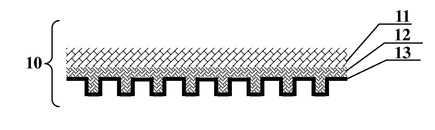
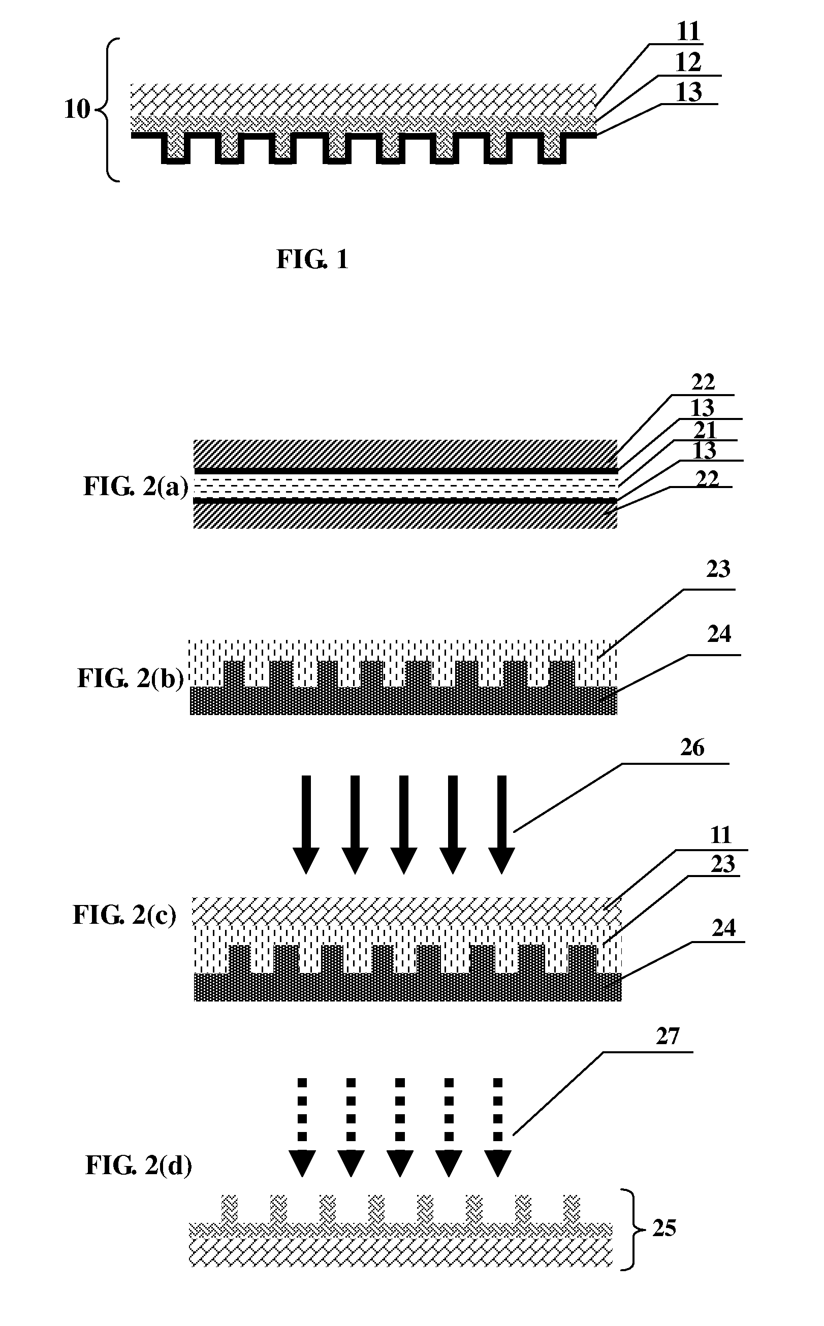
[0023]Referring to FIG. 1 for the schematic structure of a flexible mold 10 for imprinting planar and curved substrate according to a preferred embodiment of the present invention, a flexible mold 10 comprises a double-layer structure: an ultra-thin rigid patterning feature layer 12 and a thicker elastic polymer support 11. A self-assembled monolayer (SAM) 13 of trichloro-perfluoroalkyl silane is coated onto the rigid patterning feature layer 12. The thickness of the rigid patterning feature layer 12 can be adjusted from 30 nm to 500 nm according to the height of the protruding and recess features on the mold master. The thickness of the elastic polymer support 11 can be adjusted from 0.1 mm to 3 mm. The rigid patterning feature layer 12 is chemically coupled to the elastic support 11. The rigid and elastic properties of the flexible mold layers are indicated by their tensile modulus. The tensile modulus of the rigid patterning feature layer 12 is preferably more than 20 N / mm2 as a ...


PUM

PropertyMeasurementUnit
Lengthaaaaaaaaaa
Lengthaaaaaaaaaa
Pressureaaaaaaaaaa

Abstract

The present invention provides a flexible nanoimprint mold which can fabricate sub-15 nm ultra fine structures on either planar or curved substrates. The mold comprises a top ultra-thin rigid layer of imprint patterning features and a bottom thick flexible layer of polymer elastomer. The two distinct layers are preferably integrated via chemically bonding. The top layer of the mold enables a sub-15 nm resolution of pattern fabrication and the bottom layer affords a conformal contact to planar or curved surface of substrates. The methods for fabricating the same are disclosed.

Description

BACKGROUND OF THE INVENTION[0001]1. Field of the Invention[0002]The present invention relates to a nanoimprint technology, and more particularly, to a flexible imprint mold for patterning ultra-fine nanostructures on a planar or curved substrate and the method for fabricating the same.[0003]2. Description of the Related Art[0004]Nanoimprint lithography is one of the promising technologies for patterning ultra-fine nanostructures with a sub-10 nm resolution by high volume and low cost. In nanoimprint lithography, a mold with nanostructures, generally fabricated on stiff materials such as silicon, silicon dioxide, and quartz wafers, is pressed into polymer film to form relief patterns according to nanostructures of the mold. Nanoimprint lithography is described in detail in U.S. Pat. No. 5,772,905. The usual nanoimprint lithography process of pressing the mold into the thin film of thermoplastic polymer involves applying high pressure and temperature that may limit the application of ...

Claims


Application Information

Patent Timeline
IPC IPC(8): B29C59/16B29C33/38
CPCB29C33/40B82Y10/00B82Y40/00G03F7/0002B05D1/005Y10T156/1023B29K2083/00G03F1/76G03F7/20B29C33/405B29K2883/00B29C59/022
Inventor CHEN, YANFENGGE, HAIXIONGLI, ZHIWEIYUAN, CHANGSHENGLU, MINGHUI
Owner NANJING UNIV
Why Eureka
Try Eureka