
Image sensor and method for manufacturing the same

a technology of image sensor and manufacturing method, which is applied in the direction of electrical equipment, semiconductor devices, radio frequency control devices, etc., can solve the problems of inability to meet the requirements of image sensor horizontal resolution, etc., to achieve the effect of improving the integration structure of circuitry and photodiodes

Inactive Publication Date: 2010-05-13
DONGBU HITEK CO LTD
View PDF7 Cites 7 Cited by
  • Summary
  • Abstract
  • Description
  • Claims
  • Application Information

AI Technical Summary

Benefits of technology

[0008]Embodiments of the present invention provide an image sensor capable of improving an integration structure of a circuitry and a photodiode and a method for manufacturing the same.
[0010]An embodiment provides an image sensor and a method for manufacturing the same, capable of removing a plurality of metal lines from an upper portion of a photodiode, so that the distance between a photodiode and a micro-lens can be reduced to significantly reduce an optical path, thereby improving light sensitivity.
[0011]An embodiment provides an image sensor and a method for manufacturing the same, capable of improving resolution and sensitivity.

Problems solved by technology

Although disadvantages of a CCD image sensor have been overcome in the horizontal CMOS image sensor according to the related art, unsolved problems still remain in the horizontal CMOS image sensor of the related art.
However, a fill factor may be reduced, or resolution capability may be limited.
In the horizontal CMOS image sensor according to the related art, it is very difficult to optimize a process of simultaneously manufacturing the photodiode and the transistor.
However, such shallow junction is unsuitable for the photodiode.

Method used


Image

  • Image sensor and method for manufacturing the same
  • Image sensor and method for manufacturing the same
  • Image sensor and method for manufacturing the same

Examples


first embodiment

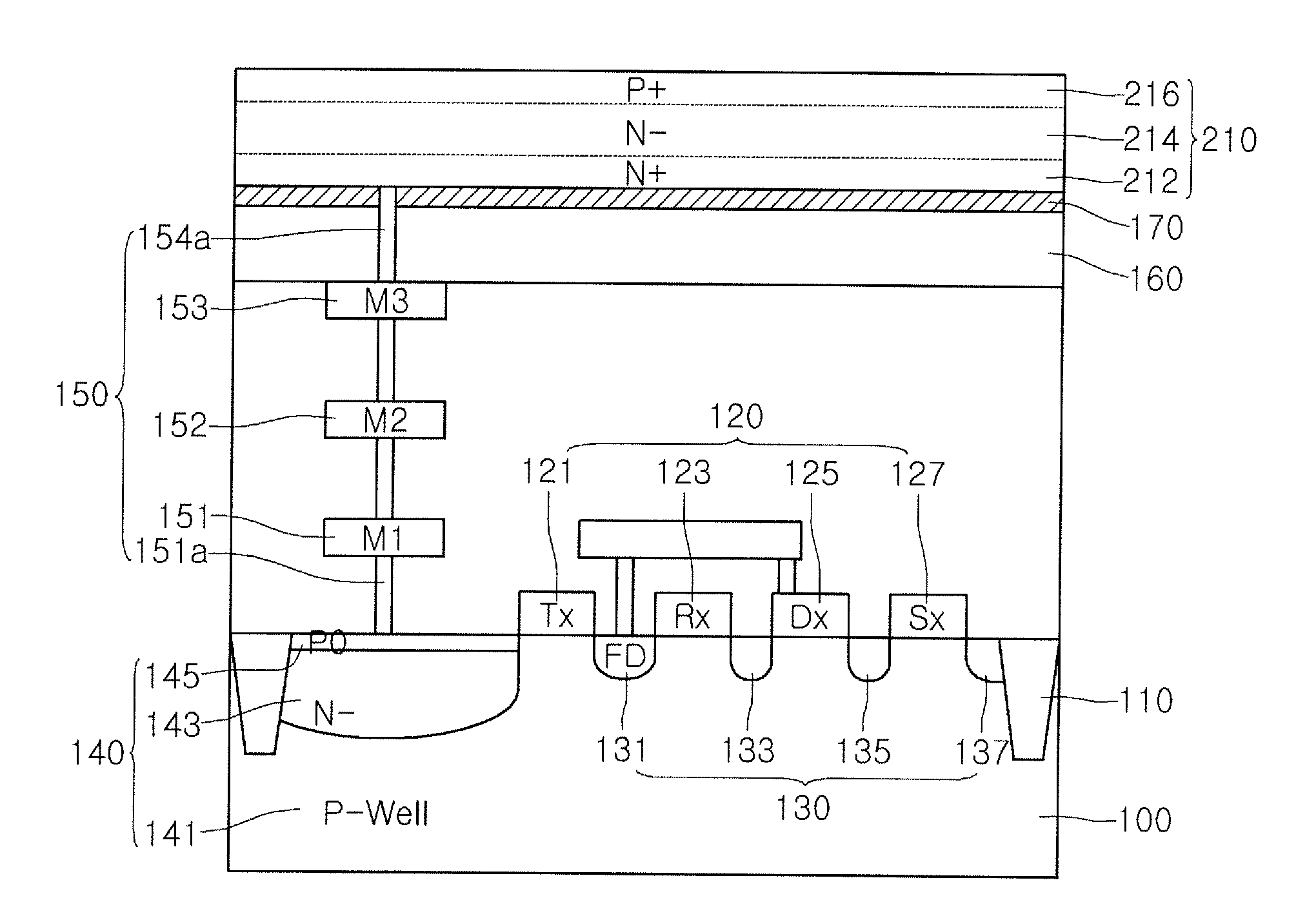
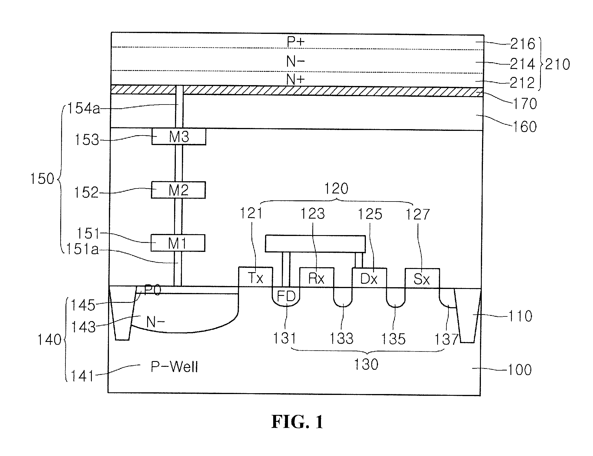
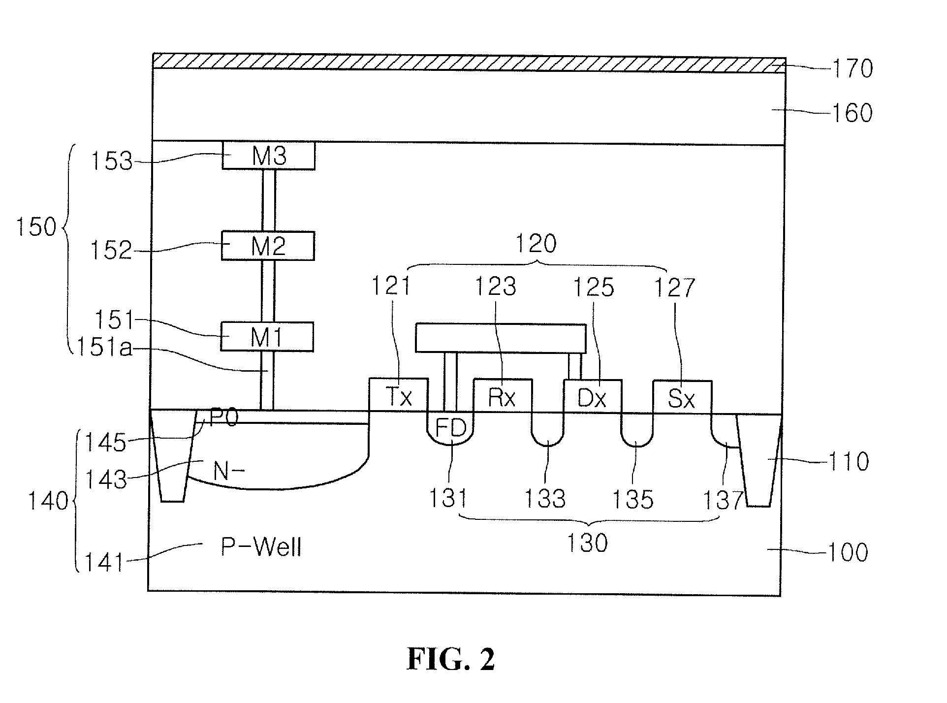
[0021]FIG. 1 is a view showing the structure of an image sensor according to a first embodiment.

[0022]The image sensor according to the first embodiment includes a first substrate 100 formed thereon with a metal line 150 and a circuitry 120, and a photodiode 210 formed over the first substrate 100 while making electrical contact with the metal line 150.

[0023]The circuitry 120 of the first substrate 100 includes an electric junction region 140 and a plurality of transistors.

[0024]The photodiode 210 may be formed in a crystalline semiconductor layer 210a (see FIG. 4). In this case, a vertical photodiode structure, in which the photodiode 210 is placed above the circuitry 120, is employed, such that the photodiode 210 is formed in the crystalline semiconductor layer. Accordingly, defects can be reduced in the photodiode 210.

[0025]Light collected (and condensed) by a micro-lens formed over the photodiode 210 may be not incident into the photodiode 210. Therefore, to improve incidence of...

second embodiment

[0057]FIG. 8 is a view showing the structure of an image sensor according to the second embodiment.

[0058]The image sensor according to the second embodiment includes the first substrate 100 formed thereon with the metal line 150 and the circuitry 120, and includes a photodiode 220 formed over the first substrate 100 while making contact with the metal line 150.

[0059]Even though a single photodiode is shown in FIG. 8 corresponding to a unit pixel, the reflective layer 170 is formed at an upper portion of metal of the metal line 150 to reflect light passing through a region between unit pixels.

[0060]The circuitry 120 of the first substrate 100 includes the electric junction region 140 and a plurality of transistors formed in the first substrate 100.

[0061]The second embodiment may employ technical features of the first embodiment.

[0062]Different from the first embodiment, the photodiode 220 may be formed on an amorphous layer according to the second embodiment.

[0063]For example, the ph...

third embodiment

[0080]FIG. 9 is a view showing the structure of an image sensor according to a third embodiment.

[0081]As shown in FIG. 9, the image sensor according to the third embodiment includes a reflective layer 370 formed on a top surface of a metal pattern to reflect light below a photodiode region.

[0082]Details the same as those of FIGS. 1 to 7 will be omitted in order to avoid redundancy except that the reflective layer 370 is formed together with the third metal 153.

[0083]The reflective layer 370 includes metal materials or non-metal materials to reflect a visible ray. After a metal layer for the third metal 153 has been formed on an interlayer dielectric layer (not shown), the reflective layer 370 is formed on the metal layer.

[0084]While forming the metal pattern by etching a portion of the metal layer, the reflective layer 370 is etched, so that the reflective layer 370 is placed on the top surface of the third metal 153.

[0085]In such an image sensor, after light incident onto a region ...


PUM


Abstract

An image sensor is disclosed that includes a first substrate including an electric junction region, a transistor, and a metal line connected to the electric junction region or the transistor; and a photodiode formed on the first substrate. The first substrate is formed at an upper portion thereof with a reflective layer to reflect light back to the photodiode.

Description

CROSS-REFERENCE TO RELATED APPLICATION[0001]This application claims the benefit under 35 U.S.C. §119 of Korean Patent Application No. 10-2008-0111416, filed Nov. 11, 2008, which is incorporated herein by reference in its entirety.BACKGROUND [0002]A CMOS image sensor according to the related art has a structure in which a photodiode and transistors are horizontally disposed.[0003]Although disadvantages of a CCD image sensor have been overcome in the horizontal CMOS image sensor according to the related art, unsolved problems still remain in the horizontal CMOS image sensor of the related art.[0004]In the horizontal CMOS image sensor according to the related art, the photodiode and the transistor are horizontally adjacent to each other on a substrate. Thus, an area for the photodiode is additionally required. However, a fill factor may be reduced, or resolution capability may be limited.[0005]In the horizontal CMOS image sensor according to the related art, it is very difficult to opt...

Claims


Application Information

Patent Timeline
IPC IPC(8): H01L31/14H01L31/18
CPCH01L27/14625H01L27/14687H01L27/14685H01L27/14632H01L27/146H01L27/14
Inventor KIM, SEOUNG HYUN
Owner DONGBU HITEK CO LTD
Learn More