Solid-state imager, method of manufacturing the same, and camera

a solid-state imager and manufacturing method technology, applied in the field of solid-state imagers, can solve the problems of low reliability, low production yield of imagers, and difficulty in insertion of optical components with high refraction index into apertures, and achieve high reliability and high production yield.

Active Publication Date: 2010-05-20
SONY SEMICON SOLUTIONS CORP
View PDF3 Cites 26 Cited by
  • Summary
  • Abstract
  • Description
  • Claims
  • Application Information

AI Technical Summary

Benefits of technology

[0012]The number of pixels in the imaging area of the solid-state imager is increasing in order to generate a high-resolution image. Compact design is also implemented in the solid-state imager. For this reason, the area of the light receiving surface of the photoelectric conversion region becomes smaller in the imaging area of the solid-state imager. An aperture for the waveguide path has a higher aspect ratio, and insertion of an optical member having a high refraction index into the aperture becomes difficult. Difficulty in constructing an appropriate waveguide path leads to low reliability and low production yield of the imagers. The production of a high-gain imager is difficult. Image quality of captured images is lowered.
[0014]It is thus desirable to provide a solid-state imager that provides high reliability and high production yield, and captures images of high image quality. It is also desirable to provide a method of manufacturing the solid-state imager and a camera including the solid-state imager.
[0029]According to embodiments of the present invention, the solid-state imager with high reliability and high production yield is provided. The camera including the solid-state imager and the manufacturing method of the solid-state imager are also provided.

Problems solved by technology

An aperture for the waveguide path has a higher aspect ratio, and insertion of an optical member having a high refraction index into the aperture becomes difficult.
Difficulty in constructing an appropriate waveguide path leads to low reliability and low production yield of the imagers.
The production of a high-gain imager is difficult.
The aspect ratio of the aperture for the waveguide path becomes substantially higher, thereby leading to the problems described above.

Method used


Image

  • Solid-state imager, method of manufacturing the same, and camera
  • Solid-state imager, method of manufacturing the same, and camera
  • Solid-state imager, method of manufacturing the same, and camera

Examples


first embodiment (

1. First Embodiment (waveguide path produced by laminating a plurality of waveguide members)

second embodiment (

2. Second Embodiment (a plurality of waveguide members joining each other at a tapered surface)

third embodiment (

3. Third Embodiment (“pupil correction” applied to a plurality of waveguide members and wiring)

4. Fourth Embodiment

5. Alternate Embodiments
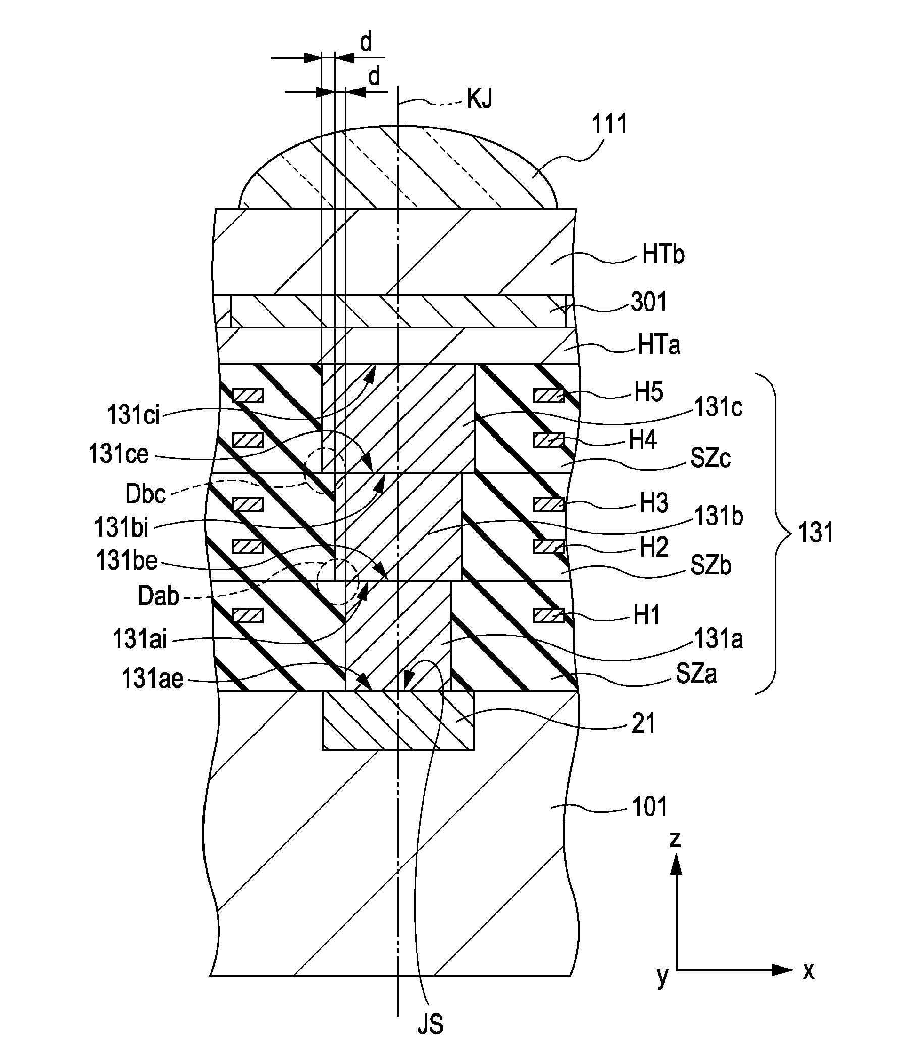
First Embodiment

Apparatus Structure

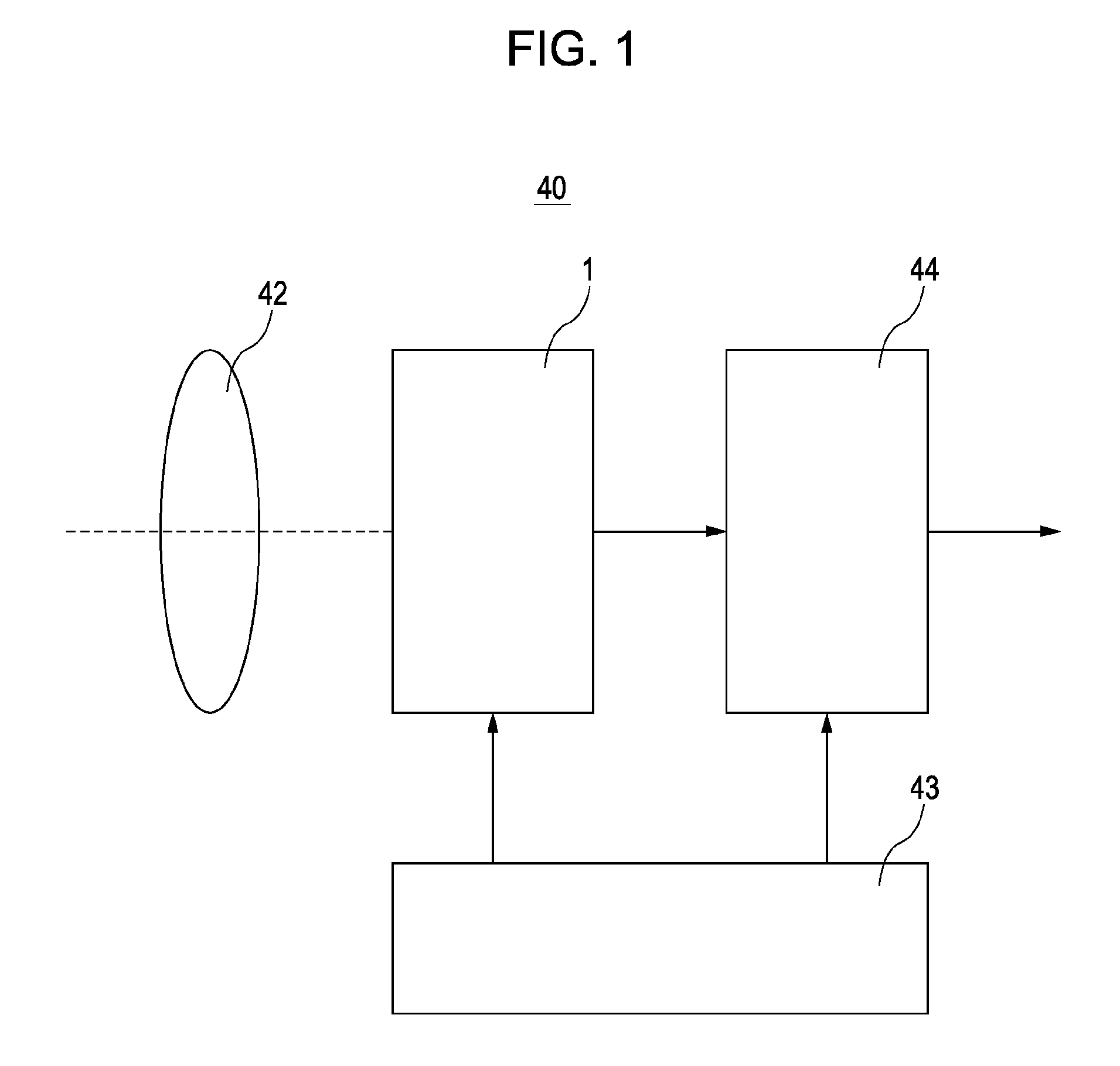
[0061]FIG. 1 illustrates the structure of a camera 40 in accordance with a first embodiment of the present invention.

[0062]The camera 40 includes solid-state imager 1, optical system 42, driver circuit 43, and signal processing circuit 44. These elements are described below.

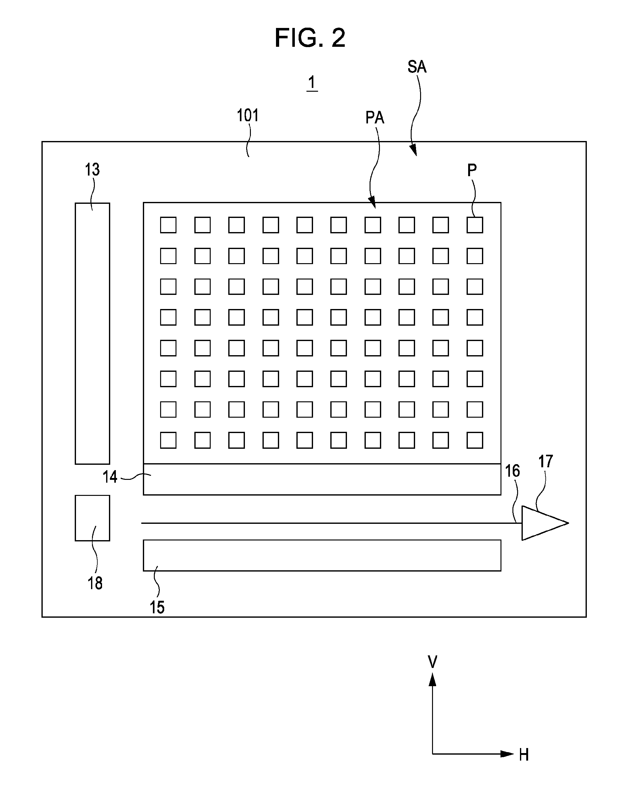
[0063]The solid-state imager 1 receives an image of a subject through the optical system 42 and photoelectrically converts light of the image of the subject into a signal charge. The solid-state imager 1 operates in response to a drive signal output from the driver circuit 43. More specifically, the solid-state imager 1 reads the signal charge and outputs the read signal charge as raw data. The solid-state imager 1 is described in detail later.

[0064]The optical system 42 including an optical lens focuses the subject image on an imaging surfac...


PUM


Abstract

A solid-state imager includes a photoelectric conversion region for photoelectrically converting a light beam received on a light receiving surface thereof into a signal charge and a waveguide path for guiding the light beam to the light receiving surface. The waveguide path includes a plurality of waveguide members, each waveguide member guiding a light beam incident on a light incident surface thereof to a light output surface thereof. The plurality of waveguide members are laminated on the light receiving surface. A first waveguide member closest to the light receiving surface from among the plurality of waveguide members faces the light receiving surface and is smaller in area than a light incident surface of a second waveguide member farthest from the light receiving surface from among the plurality of waveguide members.

Description

BACKGROUND OF THE INVENTION[0001]1. Field of the Invention[0002]The present invention relates to a solid-state imager, a method of manufacturing the same, and a camera. More specifically, the present invention relates to a solid-state imager including a photoelectric conversion region for photoelectrically converting a light beam received on a light receiving surface thereof into a signal charge, and a waveguide path for guiding the light beam to the light receiving surface. The present invention also relates to a method for manufacturing the solid-state imager and a camera including the solid-state imager.[0003]2. Description of the Related Art[0004]Cameras, such as a digital video camera and a digital still camera, include a solid-state imager. The solid-state imagers includes a complementary metal oxide semiconductor (CMOS) image sensor, and a charge-coupled device (CCD), for example.[0005]In the solid-state imager, an imaging region composed of a plurality of pixels is arranged ...

Claims


Application Information

Patent Timeline
Patent Type & Authority Applications(United States)
IPC IPC(8): H04N5/335G01J1/04H01L31/0232H01L27/14H04N5/369H04N5/374
CPCG01J1/02H04N5/335G01J1/0214G01J1/04G01J1/0422G01J1/06G01J1/4228H01L27/14605H01L27/14609H01L27/14625H01L27/14627H01L27/14629H01L27/14641H01L27/14685G01J1/0209H04N25/00G03B17/00H01L27/146
Inventor ABE, HIDESHI
Owner SONY SEMICON SOLUTIONS CORP
Why Eureka
Try Eureka