

Rotary magnet sputtering apparatus
a rotary magnet sputtering and rotary sputtering technology, applied in the direction of electrolysis components, vacuum evaporation coatings, coatings, etc., can solve the problems of degrading utilization efficiency and changing film forming rate, so as to prolong the life of the target, prevent local wear of the target, and improve the film forming rate
- Summary
- Abstract
- Description
- Claims
- Application Information
AI Technical Summary
Benefits of technology
Problems solved by technology
Method used
Image

Examples
first embodiment
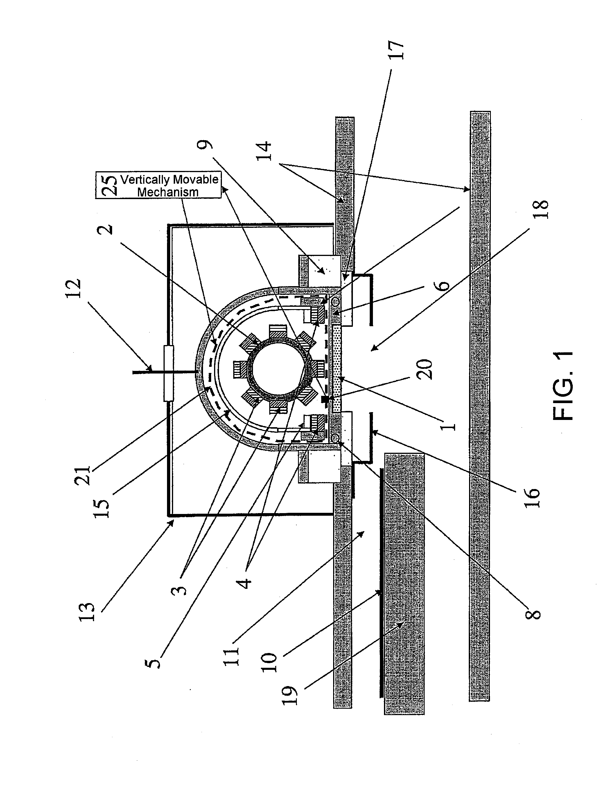
[0076]A first embodiment of this invention will be described in detail with reference to the drawings.
[0077]FIG. 1 is a sectional view for explaining the structure of a rotary magnet sputtering apparatus according to the first embodiment of this invention.
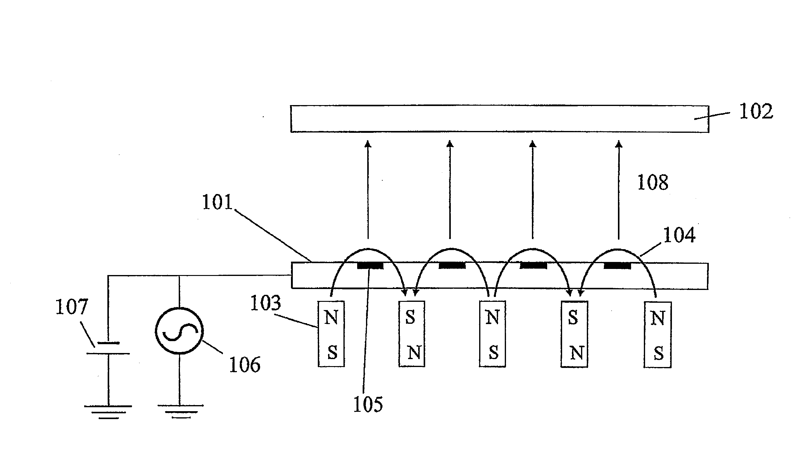
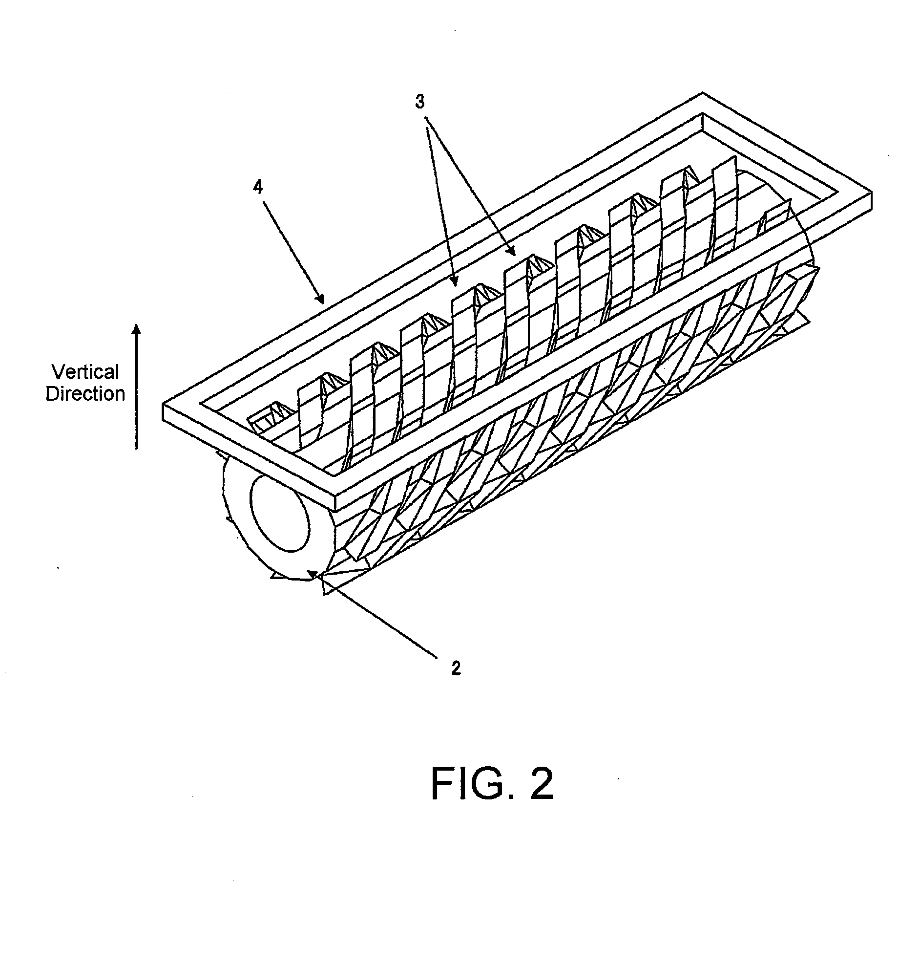
[0078]In FIG. 1, 1 denotes a target of aluminum, 2 a columnar rotary shaft, 3 a plurality of helical plate-like magnet groups (i.e., rotary magnet groups) helically disposed on a surface of the rotary shaft 2, 4 a fixed outer circumferential frame magnet disposed at the outer periphery of the rotary magnet group 3, 5 an outer peripheral paramagnetic member disposed on the side opposite to the target and faced to the fixed outer circumferential frame magnet 4, 6 a backing plate of copper to which the target 1 is bonded, 15 a paramagnetic member configured to cover the columnar rotary shaft 2 and the helical plate-like magnet groups 3 at portions thereof other than on the target side, 8 a passage for passing a coolant therethrough, 9...
second embodiment
[0100]A second embodiment of this invention will be described in detail with reference to FIG. 8. A description of portions overlapping those in the above-mentioned embodiment is omitted for brevity of description. In this embodiment, a transmitting device 801 of a semiconductor laser with visible light having a wavelength of 650 to 670 nm and a receiving device 802 of the laser are disposed outside the outer wall forming the process chamber. Laser light 804 transmitted from the transmitting device 801 is introduced into the process chamber through a viewport 803 so as to be obliquely incident on the surface of the target 1. Part of the light irregularly reflected by the surface of the target 1 reaches the receiving device 802 through another viewport 803. An angle 805 of the laser light arriving at the receiving device 802 in this event becomes smaller as the target 1 is located farther from the receiving device 802 due to consumption. Thus, it is possible to measure the distance b...
third embodiment
[0104]A third embodiment of this invention will be described in detail with reference to the following drawings. A description of portions overlapping those in the above-mentioned embodiments is omitted for simplification of description. As shown in FIG. 10, a rotary magnet sputtering apparatus according to this invention is particularly suitable when it is used as a reciprocating type film forming apparatus.
[0105]In FIG. 10, 401 denotes a process chamber, 402 a gate valve, 403 a substrate, and 404 the rotary magnet plasma excitation portion similar to the first embodiment. The axial length of the helical portion of the magnet is 2700 mm. The frequency of the plasma excitation power is set to 13.56 MHz. In terms of increasing the plasma density and reducing the plasma electron temperature, a high frequency, for example, about 100 MHz is preferable. However, the plasma excitation portion is about 2.7 m while the wavelength of 100 MHz is 3 m. If the length of the excitation portion ap...
PUM
| Property | Measurement | Unit |
|---|---|---|
| length | aaaaa | aaaaa |
| residual magnetic flux density | aaaaa | aaaaa |
| residual magnetic flux density | aaaaa | aaaaa |
Abstract
Description
Claims
Application Information