Nitride-based semiconductor laser device and optical pickup

Inactive Publication Date: 2010-05-27
SANYO ELECTRIC CO LTD
View PDF6 Cites 15 Cited by
  • Summary
  • Abstract
  • Description
  • Claims
  • Application Information

AI Technical Summary

Benefits of technology

[0040]In the aforementioned nitride-based semiconductor laser device according to the first aspect, the low refractive index layer and the high refractive index layer are preferably polycrystalline. According to this structure, an element bonding state is further strengthened in the polycrystalline state, and hence heat radiability of each

Problems solved by technology

Also in the conventional nitride-based semiconductor laser device disclosed in each of the aforementioned Japanese Patent Laying-Open Nos. 2007-059897, 2007-109737 and 2007-243023, however, deterioration or separation of the facet coating film on the light reflecting side is disadvantageously easily caused when light output is large.
In particular, deterioration of the facet coating film on a side closer to the light reflecting side facet, which has relatively large therm

Method used


Image

  • Nitride-based semiconductor laser device and optical pickup
  • Nitride-based semiconductor laser device and optical pickup
  • Nitride-based semiconductor laser device and optical pickup

Examples


Example

First Embodiment

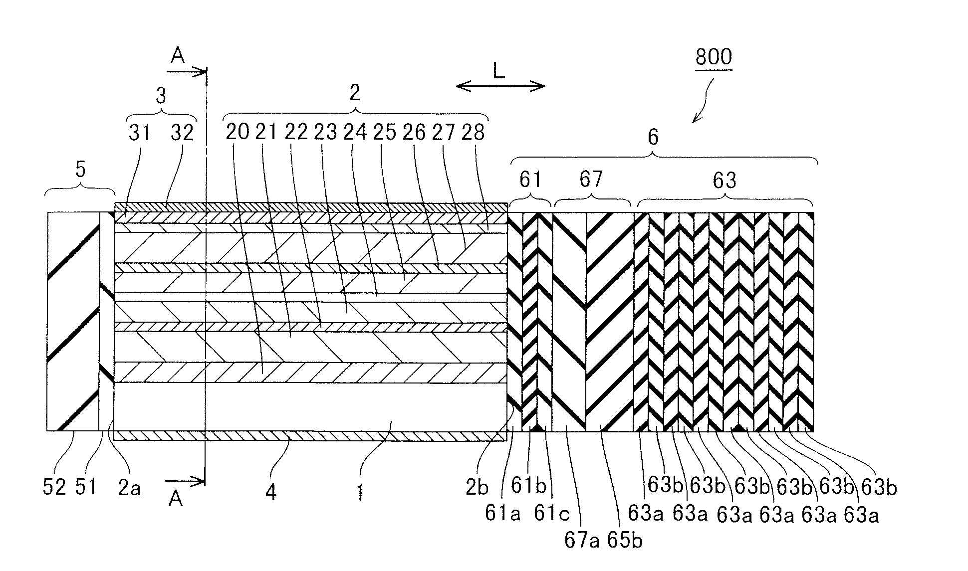
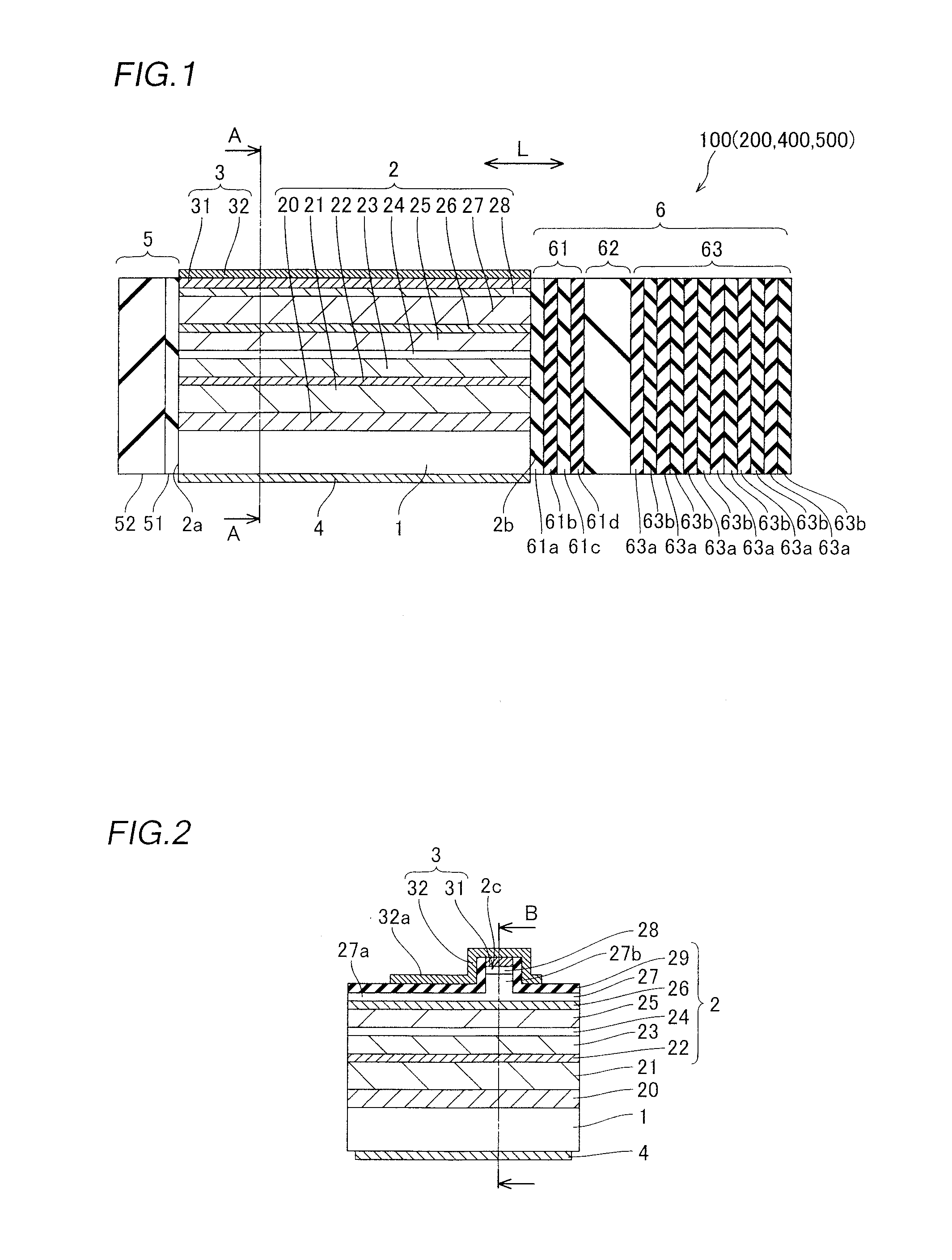
[0053]A structure of a nitride-based semiconductor laser device 100 according to a first embodiment of the present invention will be now described with reference to FIGS. 1 and 2. FIG. 1 is a sectional view of the nitride-based semiconductor laser device 100, and shows a section parallel to a laser beam emitting direction (direction L). FIG. 1 shows a section taken along the line B-B in FIG. 2.

[0054]The nitride-based semiconductor laser device 100 according to the first embodiment of the present invention has a lasing wavelength λ of about 405 nm and comprises a semiconductor element layer 2, made of a nitride-based semiconductor, formed on an upper surface ((0001) Ga plane) of a substrate 1 made of n-type GaN, a p-side electrode 3 formed on the semiconductor element layer 2 and an n-side electrode 4 formed on a lower surface ((0001) N plane) of the substrate 1, as shown in FIGS. 1 and 2. A light emitting side facet 2a and a light reflecting side facet 2b of the semi...

Example

Second Embodiment

[0091]Referring to FIG. 1, in a nitride-based semiconductor laser device 200 according to a second embodiment of the present invention, a second layer 61b in a second alteration preventing layer 61 is made of AlOxNy (where xy) having a thickness of about 30 nm, and a third layer 61c made of AlN has a thickness of about 30 nm.

[0092]The second layer 61b made of AlOxNy is formed by sputtering a Zr target by applying RF power to the Zr target while generating ECR plasma by applying microwave power in Ar, O2 and N2 gas atmosphere.

[0093]The remaining structure and manufacturing process of the nitride-based semiconductor laser device 200 are similar to those of the nitride-based semiconductor laser device 100.

[0094]According to the second embodiment, as hereinabove described, the second layer 61b in the second alteration preventing layer 61 is made of an oxynitride (AlOxNy) having a higher film density than an oxide or a nitride. Thus, a bonding state of elements is furthe...

Example

Third Embodiment

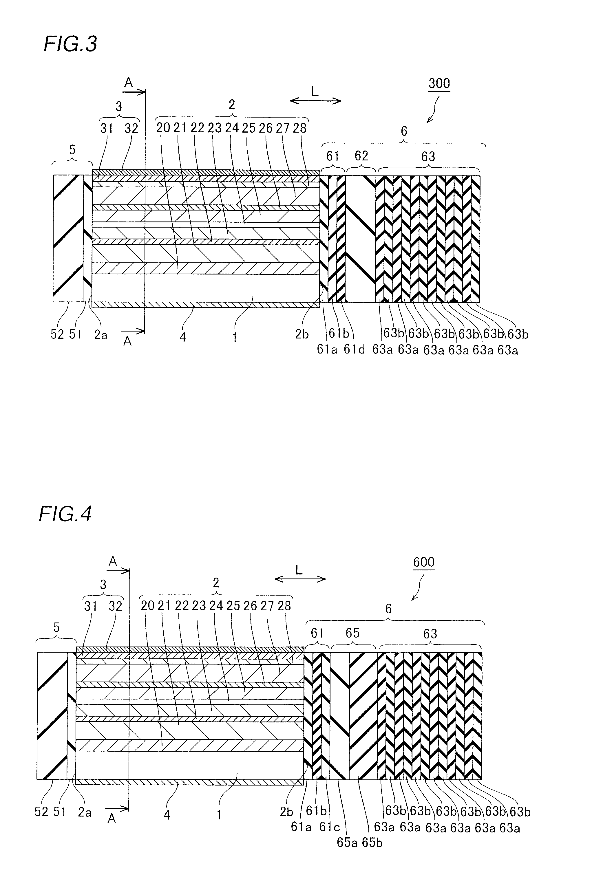
[0097]A third embodiment will be described with reference to FIGS. 1 and 3. FIG. 3 is a sectional view for illustrating a structure of a nitride-based semiconductor laser device 300 according to the third embodiment of the present invention, and shows a section parallel to an emission direction of a laser beam. The structure shown in FIG. 3 similar to that shown in FIG. 1 (first embodiment) is denoted by the same reference numerals.

[0098]In the nitride-based semiconductor laser device 300 according to the third embodiment of the present invention, a fourth layer 61d is formed directly on a second layer 61b without forming a third layer 61c in a structure of a second alteration preventing layer 61. The remaining structure and manufacturing process of the nitride-based semiconductor laser device 300 are similar to those of the nitride-based semiconductor laser device 200.

[0099]According to the third embodiment, as hereinabove described, the second alteration preventing...


PUM


Abstract

A nitride-based semiconductor laser device includes a facet coating film including an alteration preventing layer formed on a light reflecting side facet of a nitride-based semiconductor element layer and a reflectance control layer formed on the alteration preventing layer. The reflectance control layer is formed by a high refractive index layer and a low refractive index layer which are alternately stacked, the alteration preventing layer is constituted by stacking at least two layers, each of which is formed by a dielectric layer made of a nitride, an oxide or an oxynitride. The alteration preventing layer has a first layer made of a nitride in contact with the light reflecting side facet, and a thickness of each of the layers constituting the alteration preventing layer is smaller than that of the high refractive index layer and is smaller than that of the low refractive index layer.

Description

CROSS-REFERENCE TO RELATED APPLICATIONS[0001]The priority application number JP2008-298495, Nitride-Based Semiconductor Laser Device, Nov. 21, 2008, Shingo Kameyama, JP2009-256642, Nitride-Based Semiconductor Laser Device and Optical Pickup, Nov. 10, 2009, Shingo Kameyama, upon which this patent application is based is hereby incorporated by reference.BACKGROUND OF THE INVENTION[0002]1. Field of the Invention[0003]The present invention relates to a nitride-based semiconductor laser device and an optical pickup, and more particularly, it relates to a nitride-based semiconductor laser device formed with dielectric multilayer films on cavity facets and an optical pickup.[0004]2. Description of the Background Art[0005]Recently, wavelength shortening and higher output of a laser beam are desired as the light source of a high-density optical disk system, and a blue-violet semiconductor laser, having a lasing wavelength λ of about 405 nm, made of a nitride-based semiconductor material has ...

Claims


Application Information

Patent Timeline
IPC IPC(8): G01J1/20H01S5/026
CPCB82Y20/00H01S5/02212H01S5/028H01S5/0282H01S5/34333H01S5/2009H01S5/2201H01S5/305H01S5/3063H01S5/0287
Inventor KAMEYAMA, SHINGO
Owner SANYO ELECTRIC CO LTD
Why Eureka
Try Eureka