Memory device and semiconductor device

a memory device and semiconductor technology, applied in thermoelectric devices, instruments, nanoinformatics, etc., can solve the problems of data being required to be written and additionally written, and achieve the effect of reducing the size of the memory device, simplifying the process, and reducing the cost of manufacturing

Active Publication Date: 2010-06-03
SEMICON ENERGY LAB CO LTD
View PDF26 Cites 0 Cited by
  • Summary
  • Abstract
  • Description
  • Claims
  • Application Information

AI Technical Summary

Benefits of technology

[0006]As a memory circuit, a DRAM (Dynamic Random Access Memory), an SRAM (Static Random Access Memory), an FeRAM (Ferroelectric Random Access Memory), a mask ROM (Read Only Memory), an EPROM (Electrically Programmable Read Only Memory), an EEPROM (Electrically Erasable and Programmable Read Only Memory), a flash memory and the like are given. Among them, a DRAM and an SRAM are volatile memory circuits in which data is erased when the power is turned off and it is necessary to write data every time the power is turned on. An FeRAM is an involatile memory circuit; however, since it uses a capacitor element including a ferroelectric layer manufacturing steps thereof are increased. A mask ROM has a simple structure; however, data is required to be written during the manufacturing steps and cannot be additionally written. An EPROM, an EEPROM, and a flash memory are involatile memory circuits; however, an element having two gate electrodes is used, and thus, the manufacturing steps are increased.
[0021]A memory device of the present invention is capable of selectively recording and erasing data by applying voltage to a pair of conductive layers. Therefore, it is possible to write and erase data at a time other than during manufacturing by selectively heating an arbitrary memory element. Also, since there is no need to provide a separate device for writing and erasing data, the memory device can be downsized and simplified. Further, by using the present invention, a compact-sized semiconductor device can be manufactured inexpensively.

Problems solved by technology

A mask ROM has a simple structure; however, data is required to be written during the manufacturing steps and cannot be additionally written.

Method used


Image

  • Memory device and semiconductor device
  • Memory device and semiconductor device
  • Memory device and semiconductor device

Examples


embodiment mode 1

[0041]In this embodiment mode, one structural example of a memory element included in a memory device of the present invention is described with reference to drawings.

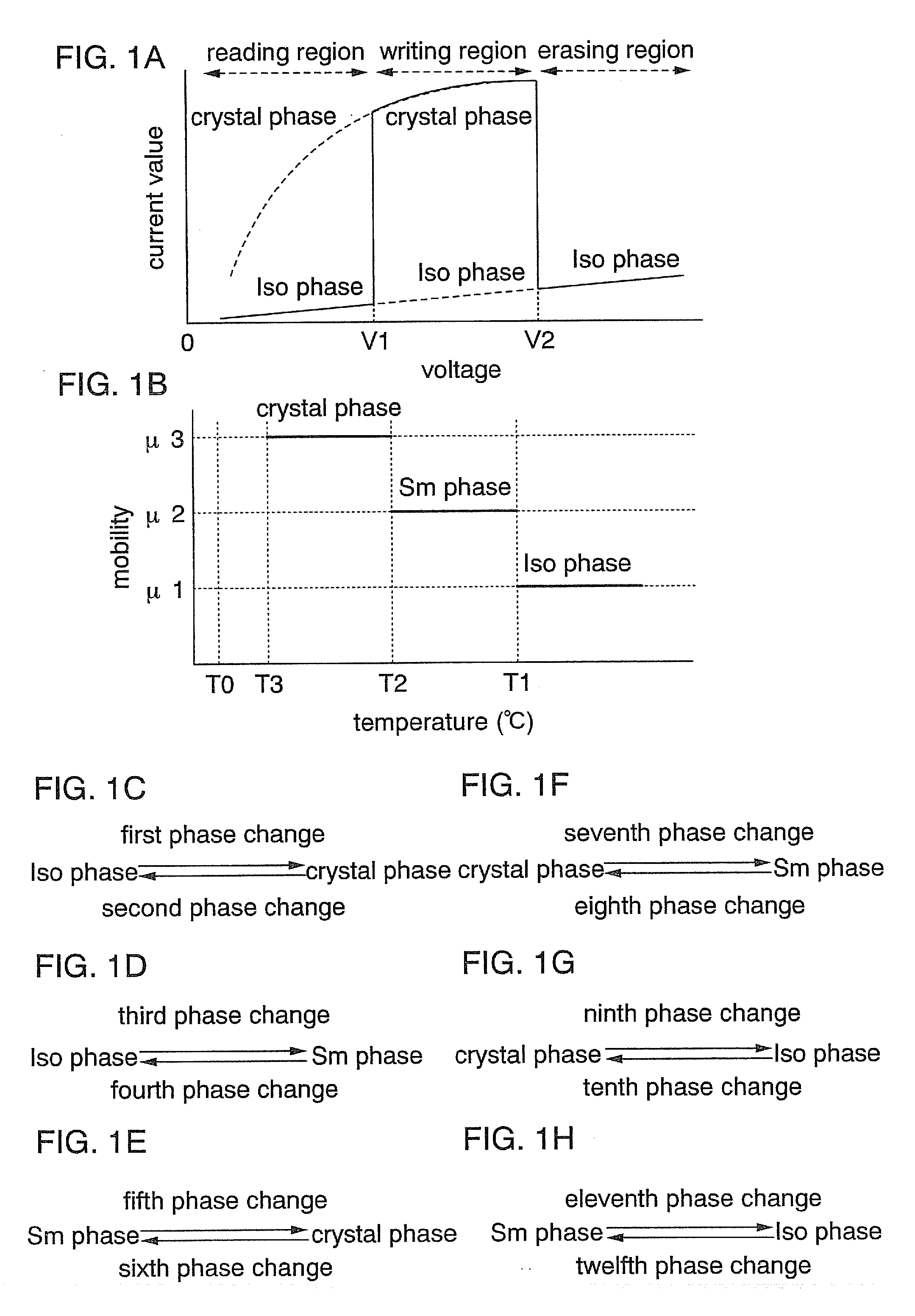
[0042]FIGS. 1A to 1H show operation methods of data reading, writing, and erasing of a memory element included in a memory device of the present invention. FIGS. 2A to 4D each show cross sectional structures of the memory elements included in the memory devices of the present invention.

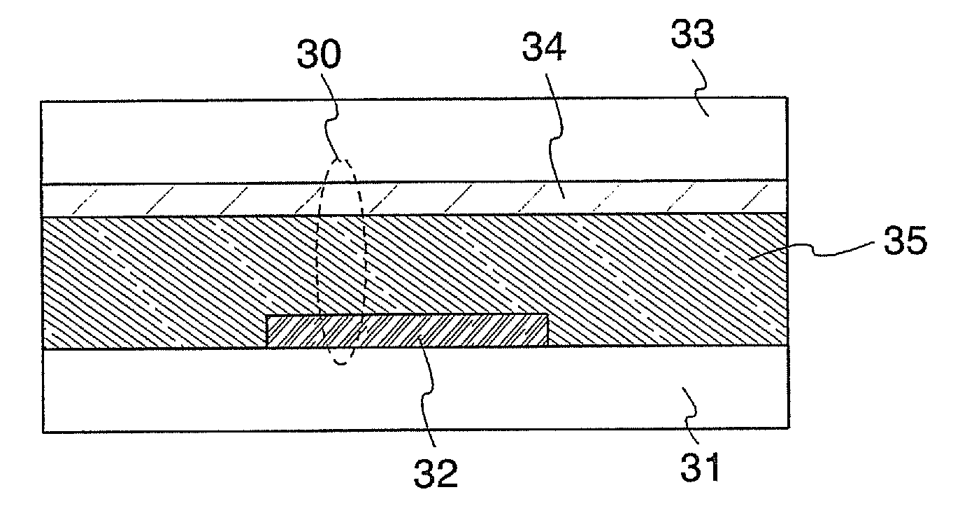
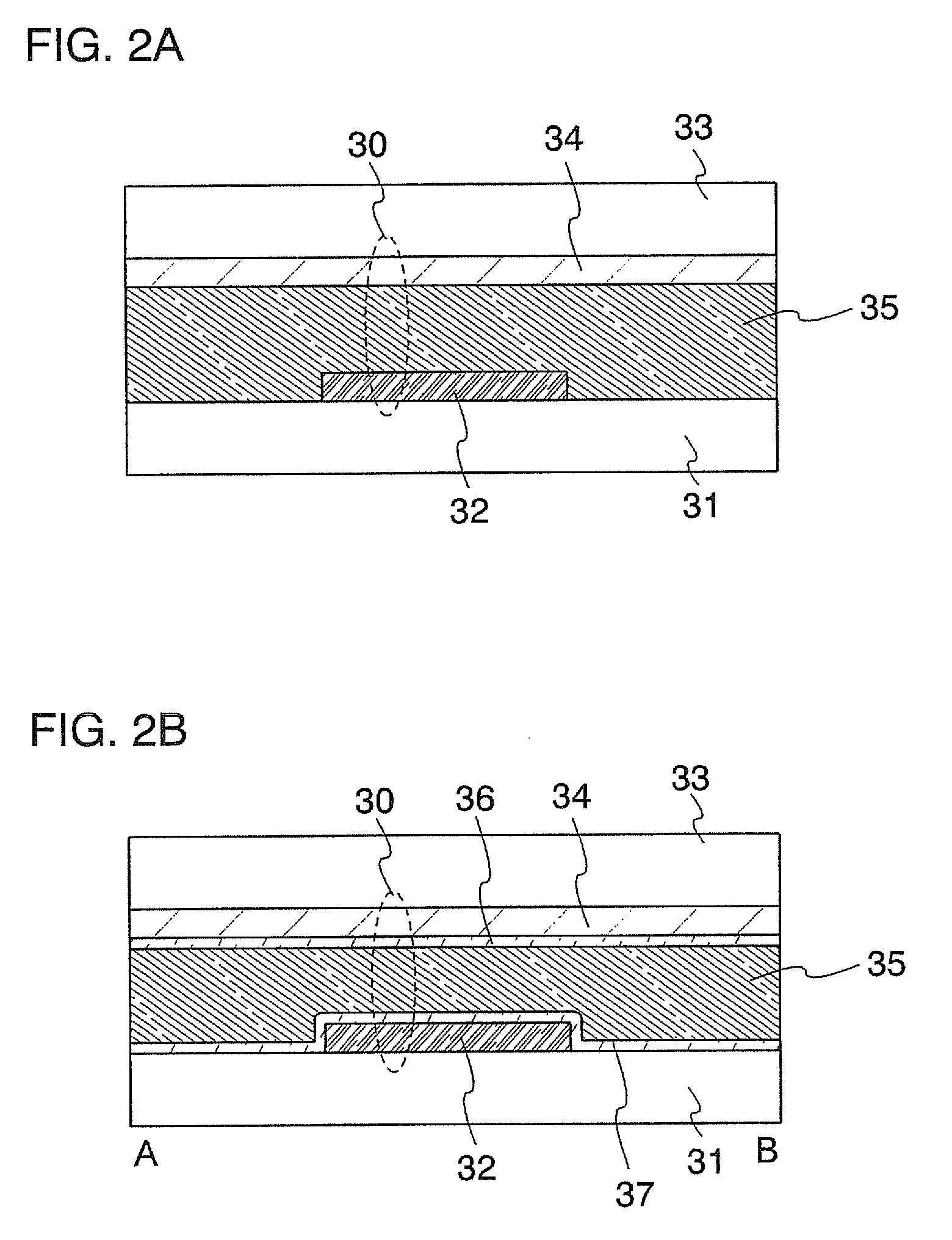
[0043]As shown in FIG. 2A, a memory element 30 includes a first conductive layer 32 fanned over a first substrate 31, a second conductive layer 34 formed adjacently to a second substrate 33, and an organic compound layer 35 interposed between the first substrate 31 and the first conductive layer 32, and the second substrate 33 and the second conductive layer 34. Also, as shown in FIG. 2B, a surface of the first substrate 31 and the first conductive layer 32, and a surface of the second substrate 33 and the second conductive layer 34 may ...

embodiment mode 2

[0090]In this embodiment mode, a structural example of a memory element that is included in a memory device of the present invention is described with reference to drawings. Specifically, a case of a passive matrix type memory device is described.

[0091]FIG. 5A shows one structural example of a memory device 16 of this embodiment mode, which includes a memory cell array 22 in which memory cells 21 are provided in a matrix form; a bit line driving circuit 26 including a column decoder 26a, a reading circuit 26b, and a selector 26c; a word line driving circuit 24 including a row decoder 24a and a level shifter 24b; an interface 23 including a writing circuit 25, an erasing circuit 27, and the like which interacts with the exterior. The writing circuit 25 and the erasing circuit 27 are each formed by a boosting circuit, a control circuit and the like. Note that, the structure of the memory device 16 shown here is only one example. Other circuits such as a sense amplifier, an output circ...

embodiment mode 3

[0110]In this embodiment mode, a memory device having a different structure from that of the above Embodiment Mode 2 is described. Specifically, a case of an active matrix type memory device is described.

[0111]A structural example of the memory device that is described in this embodiment mode is shown in FIG. 7A, which includes a memory cell array 222 in which memory cells 221 are provided in a matrix form; a bit line driving circuit 226 including a column decoder 226a, a reading circuit 226b, and a selector 226c; a word line driving circuit 224 including a row decoder 224a and a level shifter 224b; and an interface 223 including a writing circuit 227, an erasing circuit 228, and the like which interacts with the exterior. The writing circuit 227 and the erasing circuit 228 are each formed by a boosting circuit, a control circuit and the like. Note that, the structure of a memory device 216 shown here is only one example. Other circuits such as a sense amplifier, an output circuit, ...


PUM


Abstract

A memory device has a pair of conductive layers and an organic compound having a liquid crystal property that is interposed between the pair of conductive layers. Data is recorded in the memory device by applying a first voltage to the pair of conductive layers and heating the organic compound, to cause a phase change of the organic compound from a first phase to a second phase.

Description

BACKGROUND OF THE INVENTION[0001]1. Field of the Invention[0002]The present invention relates to a memory device and a semiconductor device equipped with the memory device.[0003]2. Description of the Related Art[0004]In recent years, a semiconductor device having a plurality of circuits integrated over an insulated surface and various functions has been developed. Further, development of a semiconductor device capable of wireless data transmission / reception by providing an antenna has been advanced. Such a semiconductor device is referred to as a wireless chip (also referred to as an ID tag, an IC tag, an IC chip, an RF (Radio Frequency) tag, a wireless tag, an electronic tag, or an RFID (Radio Frequency Identification) tag), and is already introduced to a part of the market.[0005]Many of these semiconductor devices that have already been put into practical use include a circuit using a semiconductor substrate such as a Si substrate (also referred to as an IC (Integrated Circuit) ch...

Claims


Application Information

Patent Timeline
Patent Type & Authority Applications(United States)
IPC IPC(8): H01L45/00H01L51/00
CPCG11C13/0069G11C2013/009H01L27/285H01L51/0035G11C13/0014B82Y10/00G11C11/5664G11C11/5678G11C13/0004H01L51/0038H10K19/202H10K85/114H10K85/111
Inventor OHSAWA, NOBUHARU
Owner SEMICON ENERGY LAB CO LTD
Why Eureka
Try Eureka