Solar Cell With Co-Planar Backside Metallization

a solar cell and co-planar technology, applied in the field of solar cell production, can solve problems such as inability to sell pads, achieve the effects of facilitating the handling of solar cells, reducing the amount of costly solder pad metal, and maximizing the exposed surfa

Inactive Publication Date: 2010-06-10
SOLARWORLD INNOVATIONS
View PDF101 Cites 4 Cited by
  • Summary
  • Abstract
  • Description
  • Claims
  • Application Information

AI Technical Summary

Benefits of technology

[0008]The present invention is directed to various solar cells and associated production methods in which backside metallization is extrusion deposited onto the backside surface of a semiconductor substrate (e.g., crystalline silicon wafer) such that upper surfaces of the back surface field (BSF) metal (e.g., Al) and the solder pad metal (e.g., AgAl) are coplanar and non-overlapping, and the two metals abut each other to form a continuous metal layer that extends over the backside surface of the substrate. In one embodiment, the solder pad metal (e.g., AgAl) extends from the planar upper surface to the backside surface of the substrate (i.e., the solder pad and BSF metals have a common thickness). In another embodiment, the solder pad metal (e.g., AgAl) is disposed over a thin layer of the BSF metal (i.e., either disposed directly on the BSF metal, or disposed on an intervening barrier layer). In both embodiments, the present invention provides a planar surface that facilitates easier handling of the solar cell (e.g., using a vacuum chuck) when compared to solar cells produced by conventional overlapping methods (described above). In addition, the present invention facilitates reduction in the amount of costly solder pad metal (i.e., Ag) by avoiding the need to overlap the solder pad metal with the BSF metal, thereby maximizing the exposed surface of the solder pad metal for soldering to metal ribbon in the production of solar cell panels, while minimizing the amount of solder pad metal that contacts the substrate surface, thereby increasing the solar cell efficiency through a reduction in surface recombination velocity.

Problems solved by technology

A potential problem with this embodiment is the diffusion of Al into the solder pad region, which, if it occurs to a sufficient extent, will render the pad unsolderable since Al is not a solderable metal.

Method used


Image

  • Solar Cell With Co-Planar Backside Metallization
  • Solar Cell With Co-Planar Backside Metallization
  • Solar Cell With Co-Planar Backside Metallization

Examples


Embodiment Construction

[0024]The present invention relates to an improvement in micro-extrusion systems. The following description is presented to enable one of ordinary skill in the art to make and use the invention as provided in the context of a particular application and its requirements. As used herein, directional terms such as “upper”, “top”, “lower”, “bottom”, “front”, “rear”, and “lateral” are intended to provide relative positions for purposes of description, and are not intended to designate an absolute frame of reference. Various modifications to the preferred embodiment will be apparent to those with skill in the art, and the general principles defined herein may be applied to other embodiments. Therefore, the present invention is not intended to be limited to the particular embodiments shown and described, but is to be accorded the widest scope consistent with the principles and novel features herein disclosed.

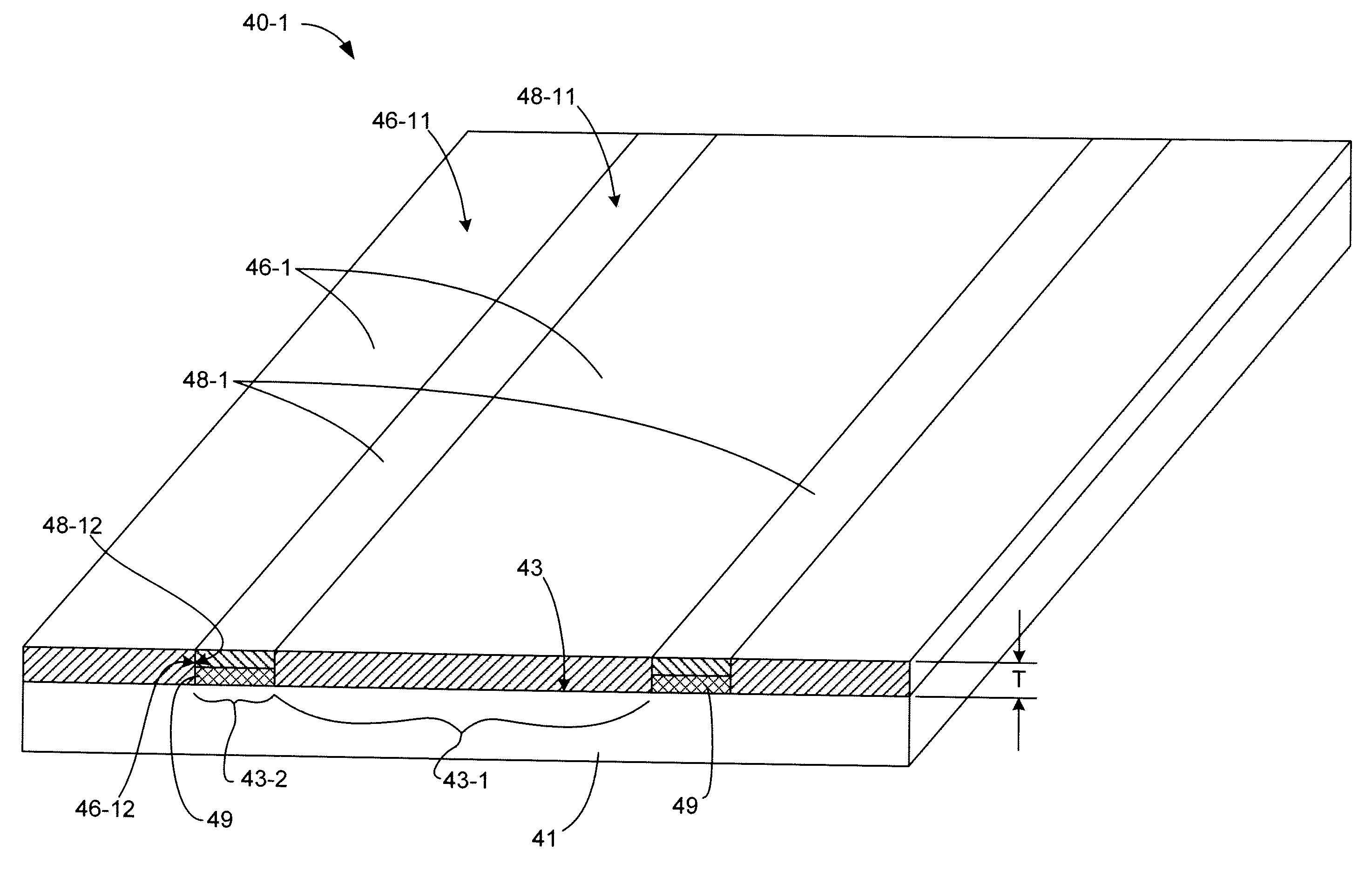
[0025]FIG. 1 is a simplified cross-sectional side view showing the backside metall...


PUM

PropertyMeasurementUnit
widthsaaaaaaaaaa
angleaaaaaaaaaa
tilted angle θ1aaaaaaaaaa

Abstract

A solar cell includes two backside metallization materials that are simultaneously extrusion deposited on a semiconductor substrate such that both a back surface field (BSF) metal layer (e.g., Al) and a solder pad metal structure (e.g., AgAl) are coplanar and non-overlapping, and the two metals abut each other to form a continuous metal layer that extends over the backside surface of the substrate. In one embodiment, the solder pad metal is formed directly on the backside surface of the substrate, either by co-extruding the two materials in the form of a continuous sheet, or by depositing spaced apart structures that are then flattened to contact each other by way of an air jet device. In another embodiment, the solder pad metal is disposed over a thin layer of the BSF metal (i.e., either disposed directly on the BSF metal, or disposed on an intervening barrier layer) using a co-extrusion head.

Description

FIELD OF THE INVENTION[0001]The present invention is related to the production of solar cells, and more particularly to the production of backside metallization on H-pattern solar cells.BACKGROUND[0002]FIG. 10 is a simplified diagram showing an exemplary conventional H-pattern contact solar cell 40 that converts sunlight into electricity by the inner photoelectric effect. Solar cell 40 is formed on a semiconductor (e.g., multi-crystalline silicon) substrate 41 that is processed using known techniques to include an n-type doped upper region 41A and a p-type doped lower region 41B such that a pn-junction is formed in the substrate 41. Disposed on a frontside surface 42 of semiconductor substrate 41 are a series of parallel metal gridlines (fingers) 44 (shown in end view) that are electrically connected to n-type region 41A. A substantially solid conductive layer 46 is formed on a backside surface 43 of substrate 41, and is electrically connected to p-type region 41B. An antireflection...

Claims


Application Information

Patent Timeline
Patent Type & Authority Applications(United States)
IPC IPC(8): H01L31/00H01L21/00H01L31/068
CPCH01L31/022425Y02E10/547H01L31/18H01L31/068H01L31/0682H01L31/04
Inventor NAKAYASHIKI, KENTAFORK, DAVID K.SOLBERG, SCOTT E.
Owner SOLARWORLD INNOVATIONS
Why Eureka
Try Eureka