Semiconductor light emitting device and method for producing the same

Inactive Publication Date: 2010-06-10
STANLEY ELECTRIC CO LTD
View PDF11 Cites 115 Cited by
  • Summary
  • Abstract
  • Description
  • Claims
  • Application Information

AI Technical Summary

Benefits of technology

[0010]According to certain aspects of the presently disclosed subject matter, the semiconductor light emitting device can maintain the high luminance (luminous flux) while suppressing the occurrence of wire breakage with high quali

Problems solved by technology

However, the greater the amount of titanium oxide contained in the sealing member, the higher the hardness of the sealing member is.
As a result, the internal stress accumulated therein due to environmental variation such as temperature variation may be inc

Method used


Image

  • Semiconductor light emitting device and method for producing the same
  • Semiconductor light emitting device and method for producing the same
  • Semiconductor light emitting device and method for producing the same

Examples


first exemplary embodiment

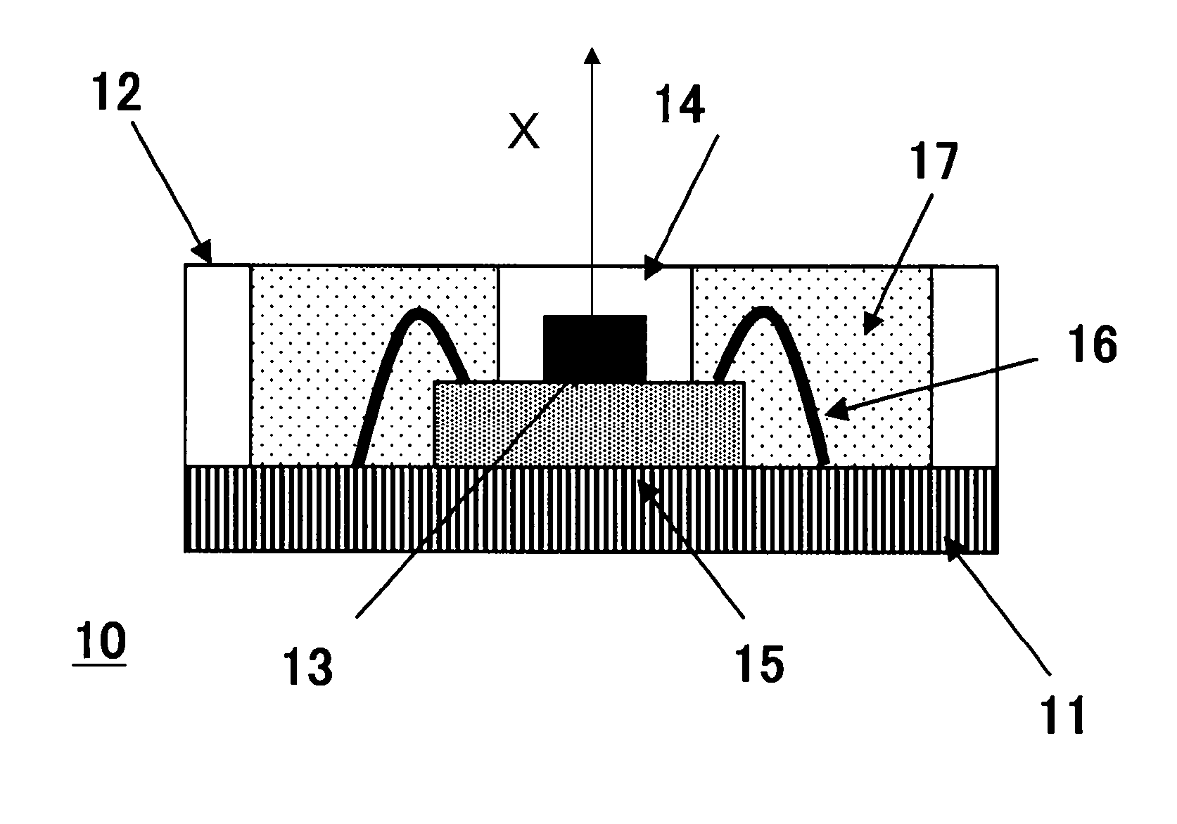
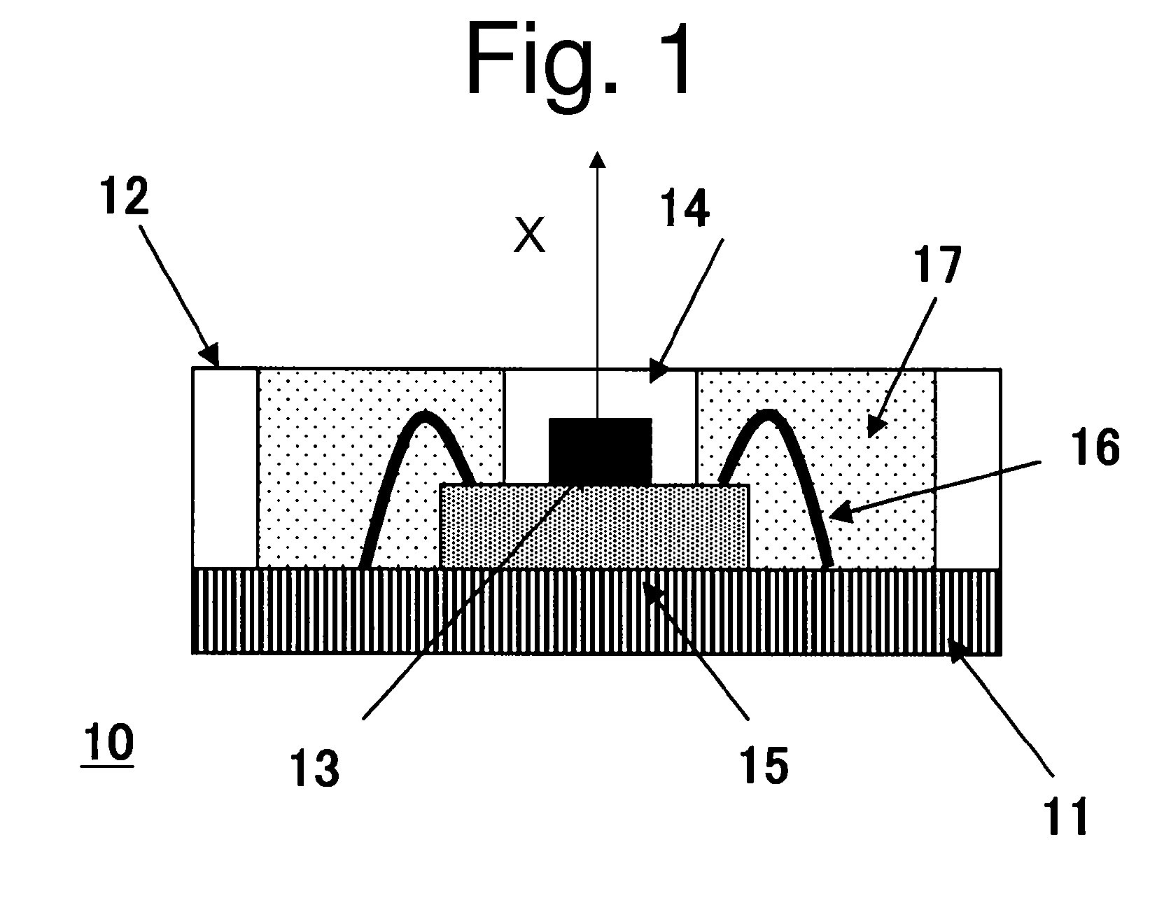
[0022]A first exemplary embodiment will be described with reference to the accompanying drawings. The same or similar components in the drawings illustrating the embodiments of the presently disclosed subject matter are denoted by the same reference numerals, and repetitive descriptions therefore will be appropriately omitted.

[0023]FIG. 1 is a cross-sectional view illustrating a semiconductor light emitting device made in accordance with the principles of the presently disclosed subject matter. As shown, the semiconductor light emitting device 10 of the presently disclosed subject matter can include: a substrate 11, a protective frame 12 disposed on the substrate 11, a semiconductor light emitting element (for example, a light emitting diode) 13, a wavelength conversion layer 14 formed so as to surround the semiconductor light emitting element 13, a submount 15 where the semiconductor light emitting element 13 and the wavelength conversion layer 14 are mounted, bonding wires (for ex...


PUM


Abstract

A semiconductor light emitting device can be configured to maintain high luminance and to suppress the possibility of the occurrence of wire breakage with high quality and reliability. A method for producing such a semiconductor light emitting device with a high process yield is also disclosed. The semiconductor light emitting device can include a sealing member into which a reflective filler can be mixed in such an amount (concentration) range that luminous flux with a predetermined amount can be maintained and the possibility of the occurrence of wire breakage can be lowered. Various sealing members containing a reflective filler with a plurality of concentrations within this range can be prepared in advance. By taking advantage of the phenomenon where chromaticity shifts depending on the concentration of the reflective filler, a semiconductor light emitting device with less chromaticity variation can be produced utilizing a sealing member with a particular concentration in accordance with the chromaticity of a particular semiconductor light emitting element that is used and which may be varied during fabrication.

Description

[0001]This application claims the priority benefit under 35 U.S.C. §119 of Japanese Patent Application No. 2008-313084 filed on Dec. 9, 2008, which is hereby incorporated in its entirety by reference.TECHNICAL FIELD [0002]The presently disclosed subject matter relates to a semiconductor light emitting device and a method for producing the same. In particular, the presently disclosed subject matter relates to a semiconductor light emitting device that is produced by resin-sealing a semiconductor light emitting element, and to a method for producing the same.BACKGROUND ART[0003]A known surface-mount semiconductor light emitting device can have a semiconductor light emitting element mounted on a submount substrate and bonding wires and the like that can be sealed with a resin-made sealing member (for example, see Japanese Patent Application Laid-Open No. 2005-026401A1). In the technique disclosed in JP 2005-026401A1 publication, it is proposed that the sealing member can function as a ...

Claims


Application Information

Patent Timeline
IPC IPC(8): H01L33/00H01L21/66
CPCH01L33/46H01L33/505H01L33/54H01L33/56H01L33/60H01L2933/0091H01L2224/48091H01L2924/3025H01L2224/45144H01L2924/00014H01L2924/00H01L33/50
Inventor HARADA, MITSUNORITACHIBANA, KAORISANMYO, MASAHIROMOCHIZUKI, MIKASATO, MASANORI
Owner STANLEY ELECTRIC CO LTD
Why Eureka
Try Eureka