Supercharge Your Innovation With Domain-Expert AI Agents!

Solid state image pickup device and camera

a pickup device and solid-state image technology, applied in the direction of cameras, instruments, printers, etc., can solve the problems of increasing chip area and power consumption, not being able to detect focus for low-contrast objects, etc., to achieve the effect of increasing the capture rate and the success rate of focus detection

Inactive Publication Date: 2010-06-10
CANON KK
View PDF16 Cites 2 Cited by
  • Summary
  • Abstract
  • Description
  • Claims
  • Application Information

AI Technical Summary

Benefits of technology

[0014]According to the present invention, specifically, a maximum value signal outputted from a photosensor array pair is level-shifted to coincide with an output reference voltage. In other words, the signal is level-shifted based on a peak reference output, and a gain is applied thereto to be outputted. FIGS. 9A and 9B show an effect of the present invention. An example shown in FIGS. 9A and 9B are cases where the peak monitor control and the peak reference output described above are combined for detecting focus of a low-contrast object. As shown in FIG. 9A, in a case of the low-contrast object, output small in amplitude is obtained from the photosensor arrays after accumulation end. However, as shown in FIG. 9B, applying a gain to the maximum value signal outputted from the photosensor array pair with reference to the output reference voltage can produce an output signal of large amplitude without exceeding a dynamic range of a gain amplifier.
[0015]According to the level shift means of the present invention, an output of large amplitude can be obtained from a low-contrast object without using a bottom detecting circuit. As a result, a capturing rate (a success rate of focus detection) can be increased.

Problems solved by technology

However, in a case where the peak monitor control and the dark reference output are used in combination to perform phase difference detecting as described above, it may not be possible to detect focus for a low-contrast object which produces a small output in amplitude.
However, according to the dark reference output described above, it may not be possible to detect focus for a low-contrast object which produces a small output in amplitude.
According to the peak bottom reference output described above, a large output in amplitude can be obtained from a low-contrast object, but a bottom detecting circuit is necessary, which increases a chip area and power consumption.

Method used


Image

  • Solid state image pickup device and camera
  • Solid state image pickup device and camera
  • Solid state image pickup device and camera

Examples


first embodiment

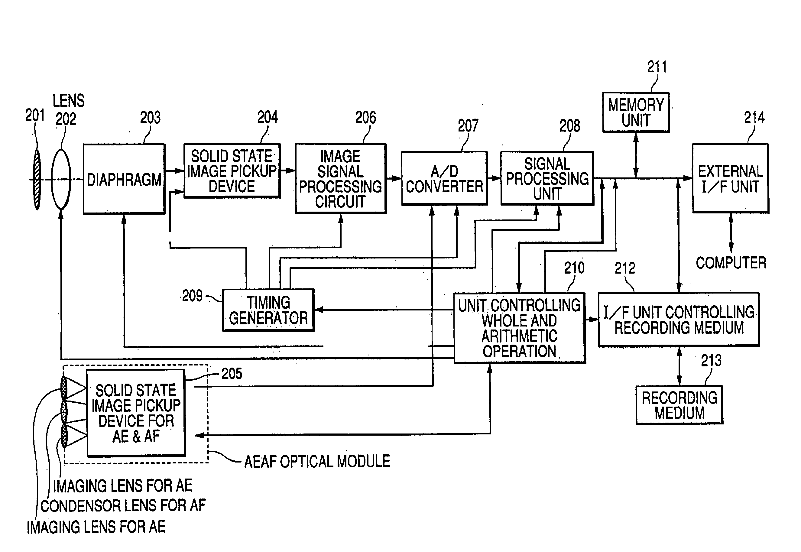
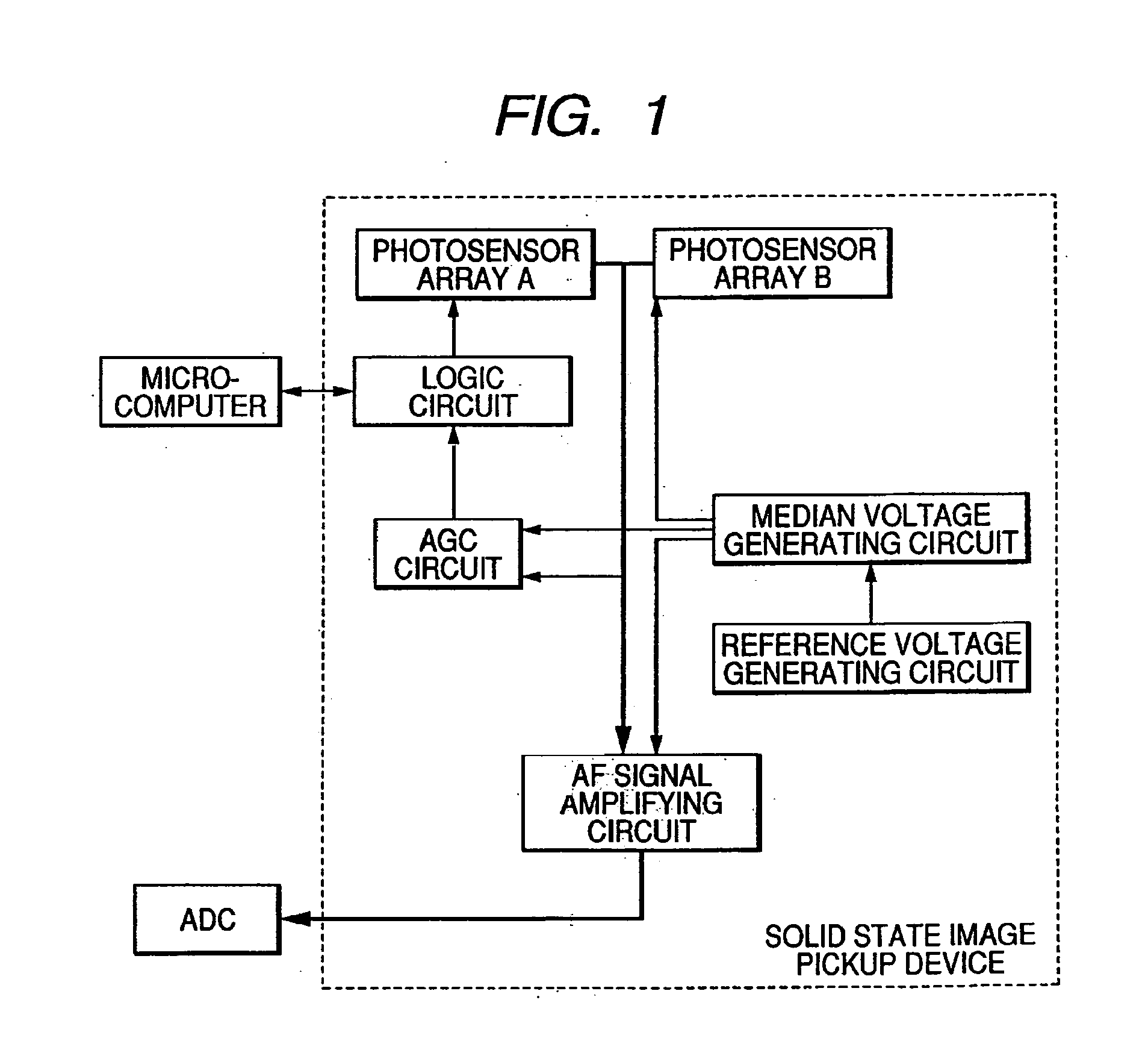
[0028]An embodiment of the present invention is described with reference to FIG. 1. FIG. 1 is a block diagram showing a solid state image pickup device for detecting focus according to a first embodiment of the present invention and an external control block.

[0029]In FIG. 1, photosensor arrays are image pickup elements each for outputting an image signal of an object. The photosensor arrays are provided in a pair, and a distance between peak signals outputted from both of the photosensor arrays is obtained to detect focus. An AF signal amplifying circuit level-shifts an output from the photosensor array and applies a gain to the level-shifted output. A reference voltage generating circuit generates a band gap reference voltage. A median voltage generating circuit generates, based on the band gap reference voltage, median voltages such as an accumulation end voltage and an output reference voltage in the solid state image pickup device. An auto gain control (AGC) circuit monitors a m...

second embodiment

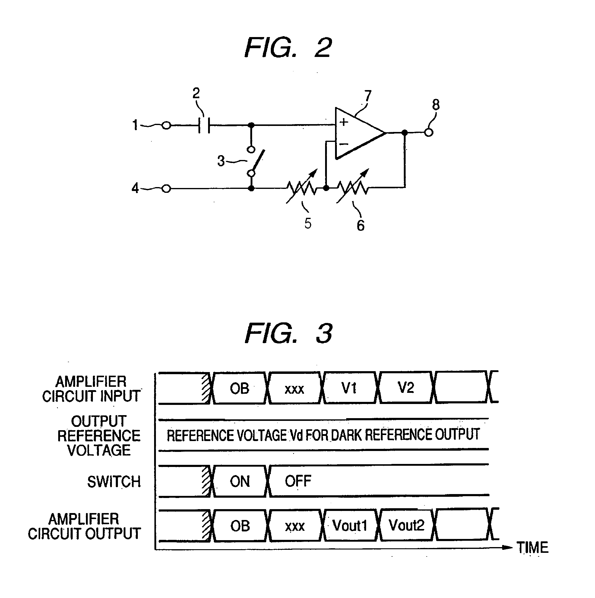
[0044]FIG. 6 is a diagram showing an AF signal amplifying circuit according to a second embodiment of the present invention.

[0045]In FIG. 6, an explanation is omitted for the components similar to those of FIG. 2. FIG. 6 shows a switch 17 which operates at the same timing of the switch 3.

[0046]The AF signal amplifying circuit according to the second embodiment can follow the operation sequence same as that of the first embodiment. The AF signal amplifying circuit according to the second embodiment is different from that of the first embodiment in that the switch 17 is additionally provided to obtain a unity gain outputted from the operational amplifier. A difference between the unity gain outputted from the operational amplifier and the output reference voltage is recorded to thereby eliminate a DC offset held by the operational amplifier.

[0047]In the second embodiment, the operational amplifier and a variable resistor are used to form the noninverting amplifier. However, the noninv...

third embodiment

[0048]FIG. 7 a diagram showing an AF signal amplifying circuit according to a third embodiment of the present invention.

[0049]In FIG. 7, an explanation is omitted for the components similar to those of FIG. 2. FIG. 7 shows variable capacitors 18 and 19 for determining an amount of gain, and a switch 20 which operates at the same timing of the switch 3. According to the first and second embodiments, a current flows between the output terminal of the operational amplifier and the input terminal 4. This current is driven by the operational amplifier and therefore relates to current consumption of the operational amplifier. Accordingly, resistance values of the variable resistors 5 and 6 of FIG. 2 must be raised in order to reduce the current consumption of the operational amplifier. However, a resistor element generally has a parasitic capacitance owing to a layout. Therefore, a greater resistance value increases an area for a layout, which increases the parasitic capacitance. As a res...


PUM


Abstract

A solid-state image pickup device wherein, in order to obtain an output of large amplitude from a low-contrast object without using a bottom detecting circuit to thereby increase a capturing rate, an accumulation end is determined when a maximum value signal in a photosensor array reaches a predetermined accumulation end level, and an amplifier circuit unit is provided for amplifying a signal, which is outputted from each of the pixels of the photosensor array, with reference to the maximum value signal of the photosensor array and for outputting the signal.

Description

BACKGROUND OF THE INVENTION[0001]1. Field of the Invention[0002]The present invention relates to a solid state image pickup device, and more particularly to a solid state image pickup device for detecting focus (hereinafter, also referred to as AF) and a camera using the solid state image pickup device for detecting focus.[0003]2. Related Background Art[0004]An explanation will be made on a conventional solid state image pickup device used for a camera for detecting focus based on a phase difference detection system. According to the conventional solid state image pickup device, an object as a subject of focus detection is projected on a photosensor array on the solid state image pickup device to obtain an electrical signal output to which photoelectric conversion has been applied, in the form of an image. Photocarrier generated in the photosensor array is subjected to charge-voltage conversion to be stored in a capacitor for holding a signal. During accumulation processing, auto ga...

Claims


Application Information

Patent Timeline
Patent Type & Authority Applications(United States)
IPC IPC(8): H04N5/335G02B7/28G02B7/30G03B13/36H04N5/232
CPCG02B7/36H04N5/353H04N5/243H04N5/23212H04N23/672H04N23/76H04N25/53
Inventor KINUGASA, TOMOHISATAKAHASHI, HIDEKAZU
Owner CANON KK
Features
  • R&D
  • Intellectual Property
  • Life Sciences
  • Materials
  • Tech Scout
  • Unparalleled Data Quality
  • Higher Quality Content
  • 60% Fewer Hallucinations
Learn More