Solar cell having nanodiamond quantum wells

a quantum well and solar cell technology, applied in the field of nanodiamond materials, can solve the problems of performance, cost, manufacturability, other factors, and other factors, and achieve the effect of improving energy conversion

Inactive Publication Date: 2010-06-17
SUNG CHIEN MIN
View PDF8 Cites 9 Cited by
  • Summary
  • Abstract
  • Description
  • Claims
  • Application Information

AI Technical Summary

Benefits of technology

[0006]The various layers of the solar cells of the present invention can be of a variety of thicknesses and configurations depending on the materials used and the intended use of the device. For example, in one aspect the doped amorphous diamond layer has a thickness of less than about 250 nanometers. In another aspect, the nanodiamond layer has a thickness of less than about 150 nanometers. In yet another aspect, the doped silicon layer is a P-type material and the doped amorphous diamond layer is an N-type material. In a further aspect, the second conductor comprises a doped portion of the amorphous diamond layer. In another aspect, at least one of the first conductor and the second conductor is transparent.
[0007]The present invention additionally provides methods for making solar cells having improved energy conversion. In one aspect, such and aspect can include forming a doped silicon layer on a substrate, depositing a nanodiamond layer on the silicon layer, and depositing a doped amorphous diamond layer on the nanodiamond layer. In one aspect the silicon layer is an amorphous silicon layer. In another aspect, the silicon layer is N-type doped and the amorphous diamond layer is P-type doped. In yet another aspect, the silicon layer is P-type doped and the amorphous diamond layer is N-type doped. In a further aspect, the silicon layer is a thin-film silicon layer.

Problems solved by technology

While much success has been obtained using amorphous diamond materials in various generating devices, drawbacks in performance, manufacturability, cost, and other factors have remained.

Method used


Image

  • Solar cell having nanodiamond quantum wells
  • Solar cell having nanodiamond quantum wells
  • Solar cell having nanodiamond quantum wells

Examples


example 1

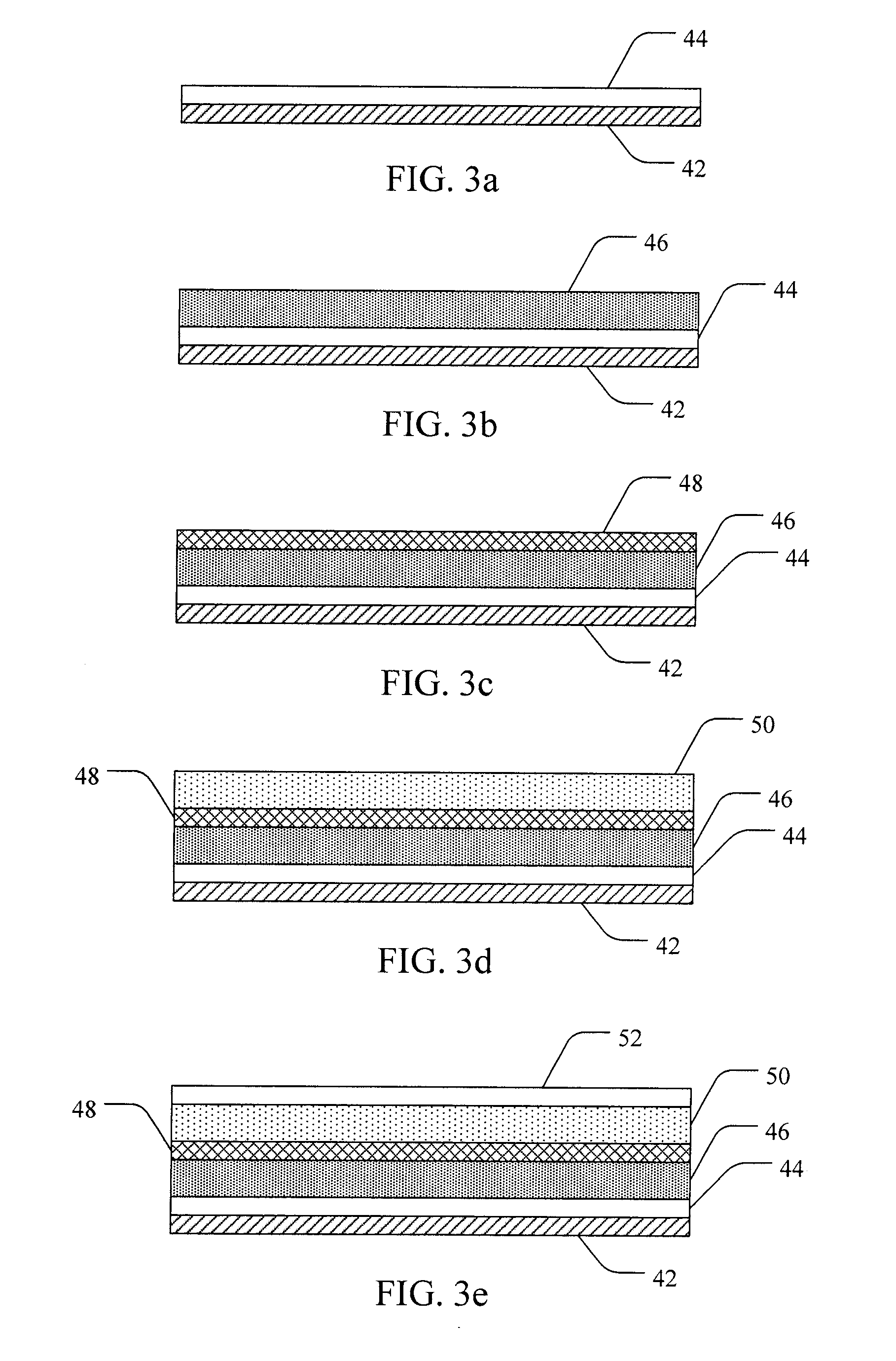
[0066]A semiconductor device is constructed as follows:

[0067]Nanodiamond is produced by detonation of dynamite (TNT+RDX) in an oxygen deficiency container, resulting in nanodiamond particles having a size range of 4-10 nm. The purified nanodiamond is dispersed in an organic binder and dried to form a layer. The layer of nanodiamond is then used as a target for magnetron sputtering with argon ions.

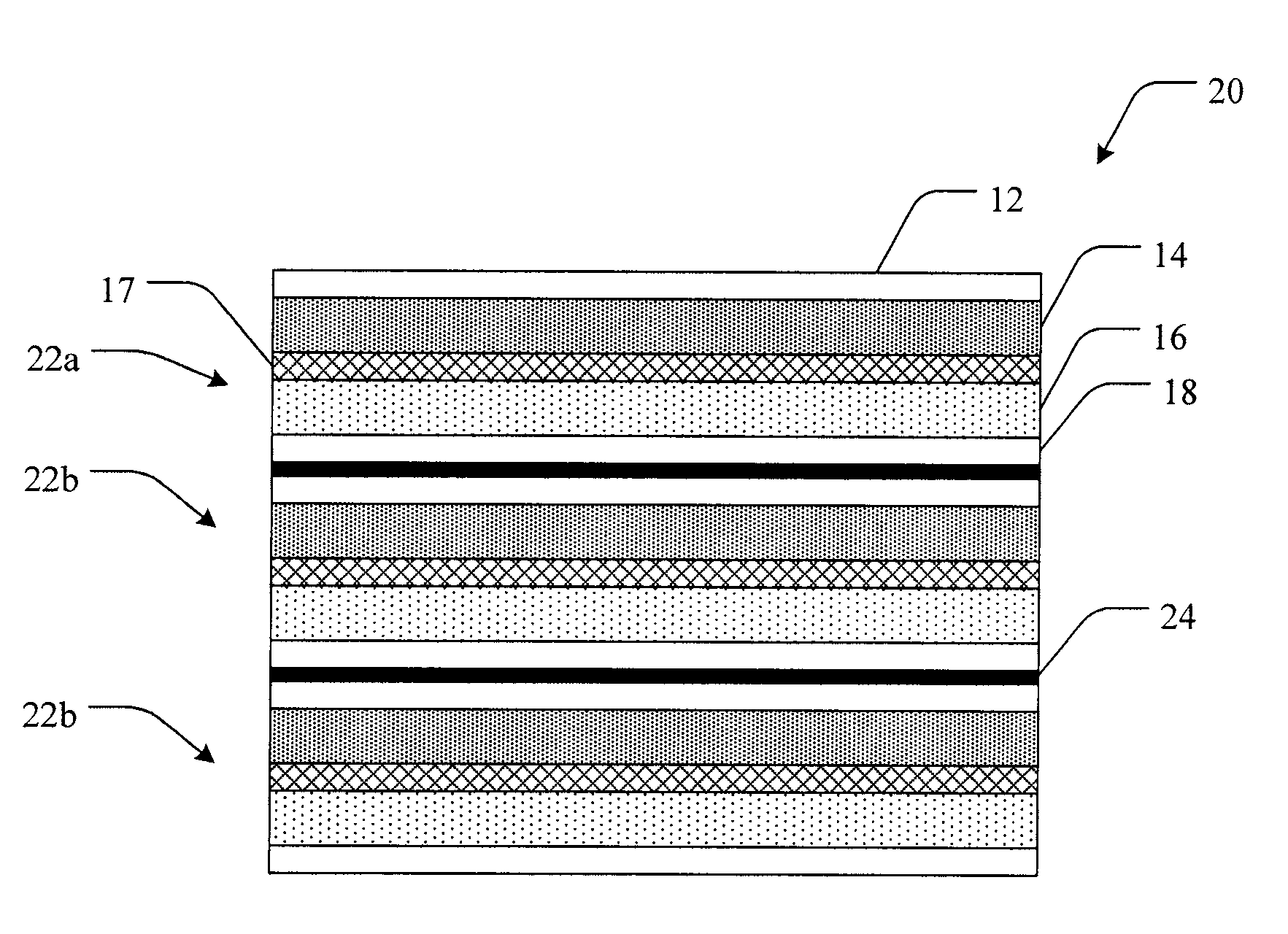
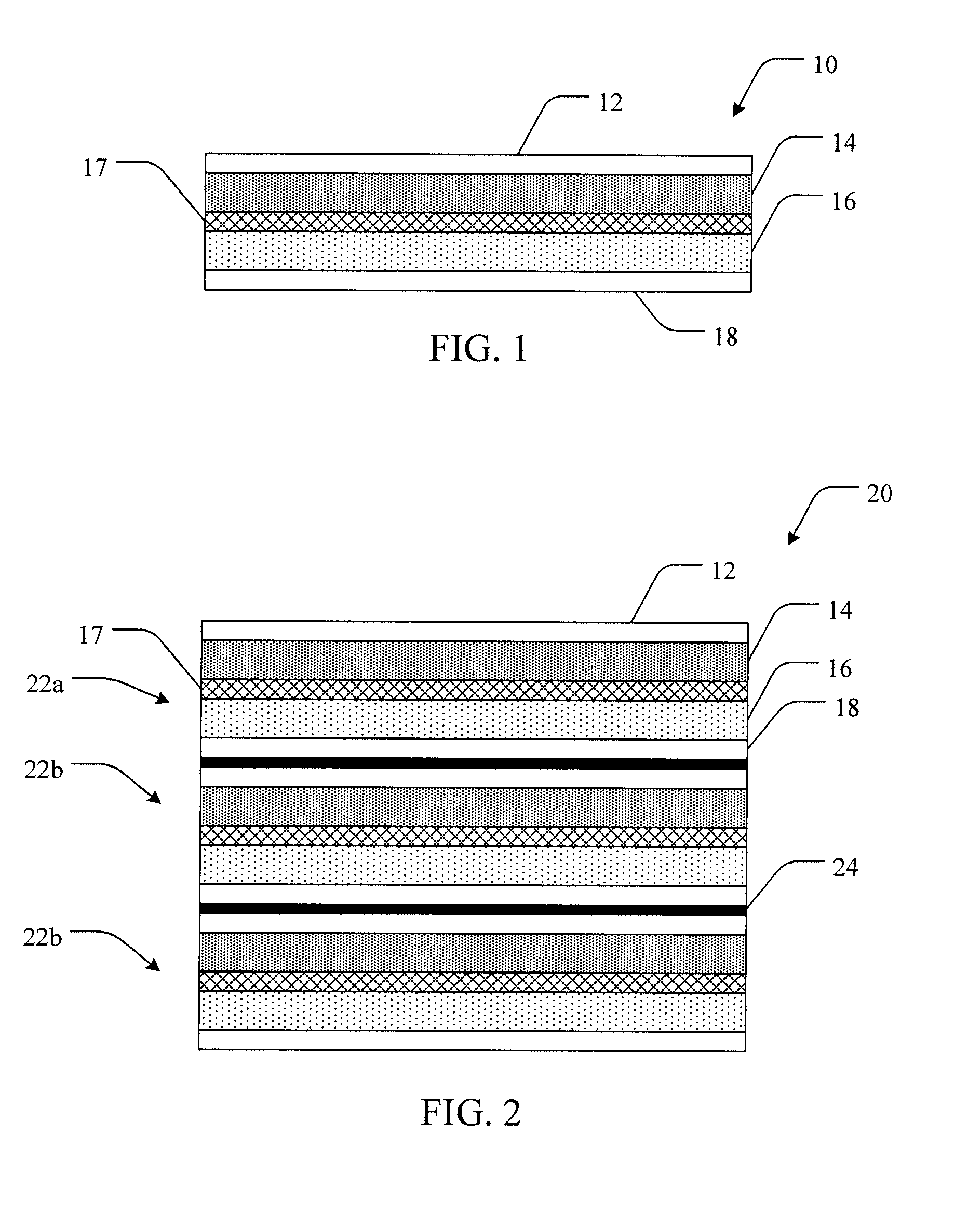
[0068]A P type silicon wafer is used as substrate that is bombarded by the sputtered diamond to form clusters of atoms. The coated P type silicon wafer is then overcoated with N type silicon to form a PIN junction suitable for use as a solar cell.

example 2

[0069]A semiconductor device as in Example 1, except the P type semiconductor is CIGS and the N type semiconductor is CdS.

example 3

[0070]A semiconductor device as in Example 1, except the P type semiconductor is boron doped amorphous diamond and the N type semiconductor is nitrogen doped amorphous diamond.


PUM

PropertyMeasurementUnit
thicknessaaaaaaaaaa
thicknessaaaaaaaaaa
bond lengthaaaaaaaaaa

Abstract

The present invention provides materials, devices, and methods for generation of electricity from solar power. In one aspect, the present invention includes a solar cell, including a first conductor, a doped silicon layer in electrical communication with the first conductor, a nanodiamond layer in contact with the doped silicon layer, a doped amorphous diamond layer in contact with the nanodiamond layer, and a second conductor in electrical communication with the doped amorphous diamond layer.

Description

PRIORITY DATA[0001]This application claims the benefit of U.S. Provisional Patent Application Ser. No. 61 / 122,239 filed on Dec. 12, 2008, and of U.S. Provisional Patent Application Ser. No. 61 / 138,429, filed on Dec. 17, 2008, each of which is incorporated herein by reference.FIELD OF THE INVENTION[0002]The present invention relates generally to devices and methods for generating electrical power, including in particular the use of nanodiamond materials. Accordingly, the present application involves the fields of physics, chemistry, electricity, and material science.BACKGROUND OF THE INVENTION[0003]Solar cell technology has progressed over the past several decades resulting in a significant contribution to potential power sources in many different applications. Despite dramatic improvements in materials and manufacturing methods, solar cells still have conversion efficiency limits well below theoretical efficiencies, with current conventional solar cells having maximum efficiency of ...

Claims


Application Information

Patent Timeline
Patent Type & Authority Applications(United States)
IPC IPC(8): H01L31/00H01L31/18H01L31/042H01L29/16
CPCB82Y20/00H01L31/035245H01L31/076Y02E10/548H01L21/02381H01L21/02444H01L31/202H01L21/02527H01L21/02592H01L31/03762H01L31/03921H01L31/0747H01L21/02513Y02E10/547Y02P70/50
Inventor SUNG, CHIEN-MIN
Owner SUNG CHIEN MIN
Why Eureka
Try Eureka