

Titanium silicon nitride deposition
a technology of titanium silicon nitride and nitride, which is applied in the direction of chemical vapor deposition coating, coating, electrical equipment, etc., can solve the problems of device reliability, among other things, that are unsatisfactory
- Summary
- Abstract
- Description
- Claims
- Application Information
AI Technical Summary
Benefits of technology
Problems solved by technology
Method used
Image

Examples
example 1
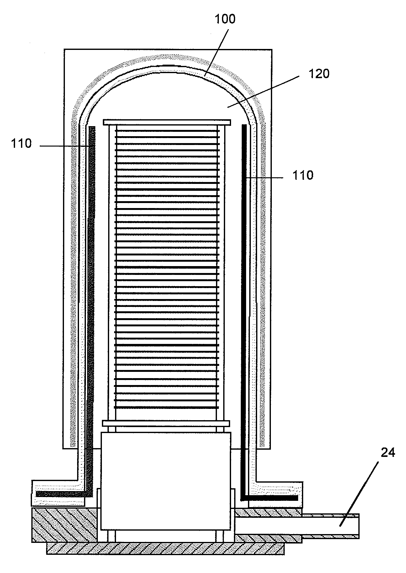
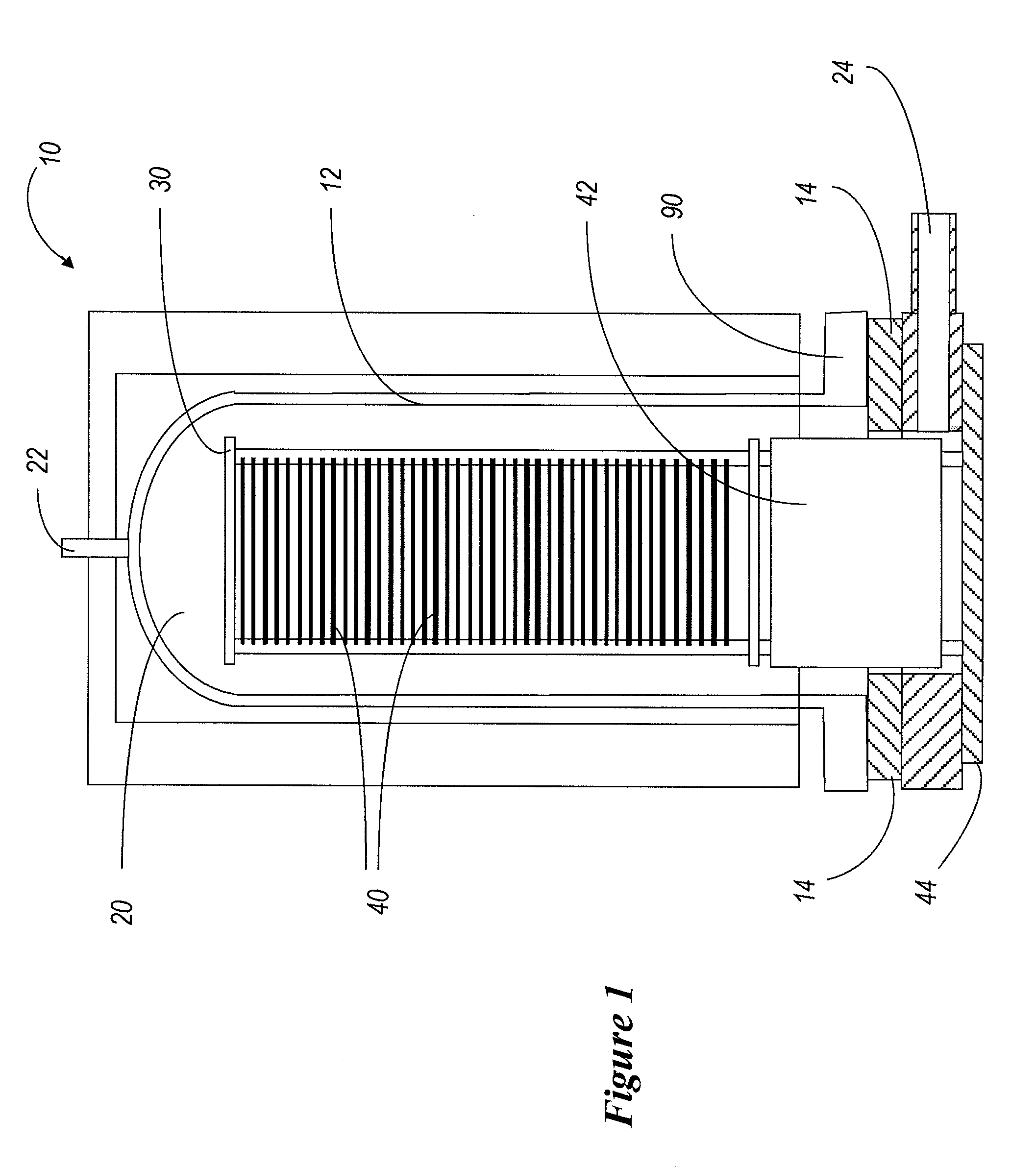
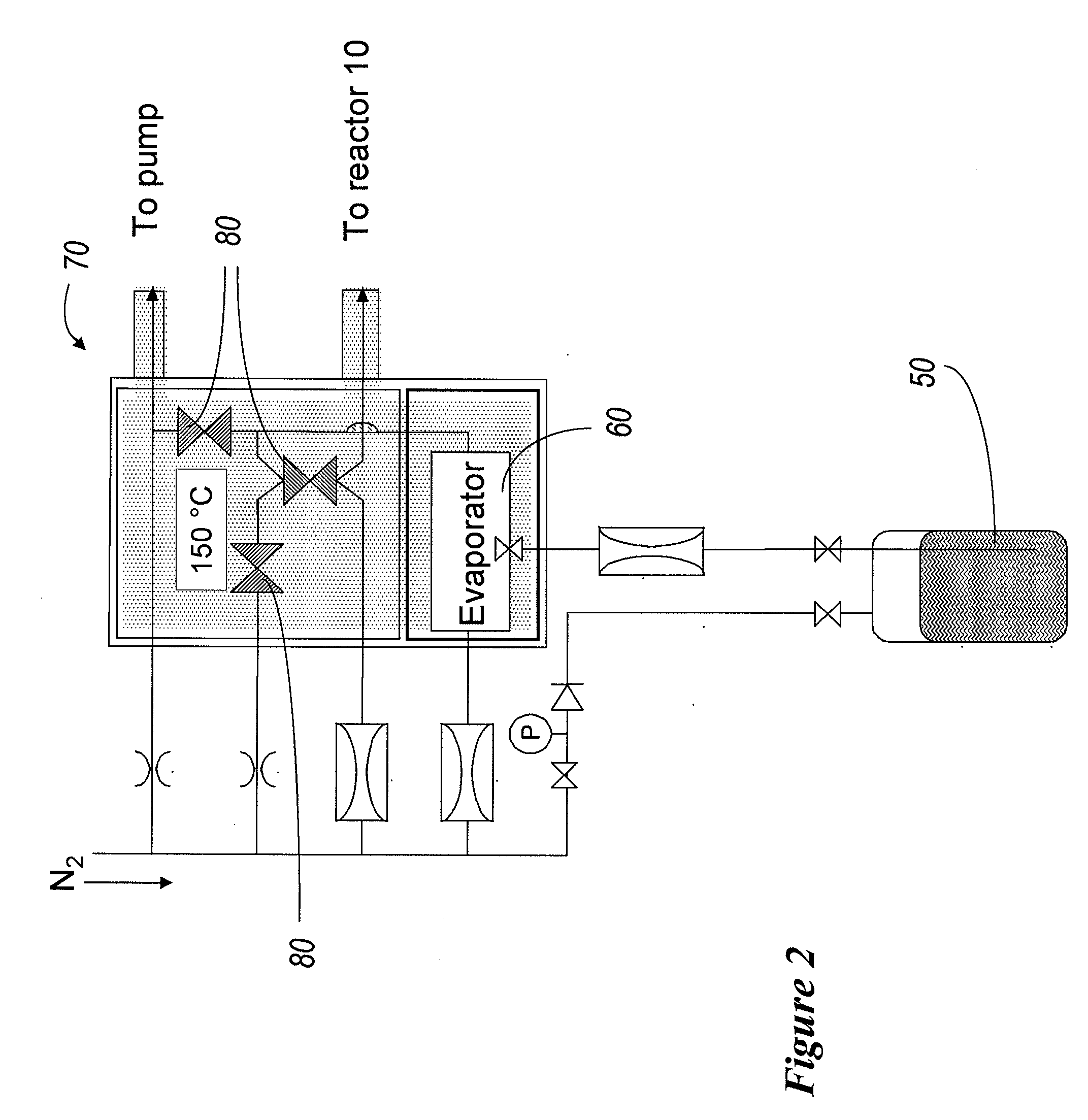
[0052]Titanium silicon nitride films were formed in an A412™ vertical furnace, commercially available from ASM International, N.V. of Bilthoven, the Netherlands. The furnace was set-up using the reactor hardware configuration of FIG. 3 and a TiCl4 liquid flow control and evaporation unit according to FIG. 2.
[0053]Substrates were loaded into a reaction chamber of the furnace. TiCl4, NH3, and SiH4 were sequentially pulsed into the reaction chamber. Each reactant was flowed into the reaction chamber of the furnace using a vertically extending multi-hole injector. The substrates were subjected to 35 deposition cycles at 500° C. and a pressure of 220 mTorr. Each cycle included the following steps:[0054]1) a TiN deposition using TiCl4 and NH3;[0055]2) a reaction chamber purge using N2;[0056]3) a reaction chamber flush using NH3 flowed at a rate greater than the flow rate of NH3 during the TiN deposition;[0057]4) a reaction chamber flush using SiH4; and[0058]5) a reaction chamber purge usi...
example 2
[0063]Titanium silicon nitride films were formed as in Example 1 above, except that the duration of the SiH4 flush was increased to 90 s. The flow rates and durations of each of steps 1)-5) are given in Table 2 below. The longer silicon precursor flush resulted in an increased sheet resistance relative to the TiSiN films of Example 1 and higher film thickness. The resulting TiSiN films have an average sheet resistance of about 3064.4 Ω / sqr and an average thickness of about 205 Å. The deposition rate was about 1.46 Å / min.
TABLE 2DepositionTiCl4SiH4NH3N2DurationStep(g / min)(sccm)(sccm)(sccm)(sec.)TiCl4 + NH32.34019070028N2-purge00040030NH3 flush00100030060SiH4 flush0400040090N2-purge200040030
[0064]It will be appreciated that the resistivity of the deposited TiSiN can be tuned by changing the amount of silicon in the TiSiN film. For example, increasing the number of sub-cycles of silicon precursor, or increasing the duration of silicon precursor exposure relative to the TiN deposition pr...
PUM
| Property | Measurement | Unit |
|---|---|---|
| temperature | aaaaa | aaaaa |
| deposition temperature | aaaaa | aaaaa |
| diameter | aaaaa | aaaaa |
Abstract
Description
Claims
Application Information