Method of thinning a semiconductor substrate

a technology of thinning and semiconductor substrates, applied in the direction of semiconductor devices, semiconductor/solid-state device details, electrical equipment, etc., can solve the problems of high processing cost, extraordinary processing sequences of semiconductor substrates, and the success of thinning a semiconductor substrate containing c4 balls in the industry, so as to reduce the adhesive strength of the adhesive tape

Active Publication Date: 2010-06-24
IBM CORP
View PDF10 Cites 19 Cited by
  • Summary
  • Abstract
  • Description
  • Claims
  • Application Information

AI Technical Summary

Benefits of technology

[0042]deactivating the adhesive tape, whereby adhe

Problems solved by technology

Since a typical semiconductor substrate as manufactured in a normal semiconductor processing sequence has a thickness from about 500 μm to about 1,000 μm, formation of through-wafer vias (TWVs) that extend through the entirety of the thickness of the semiconductor substrate requires extraordinary processing sequences and high processing cost.
While desirable for enabling chip stacking with through-wafer vias (TWVs) having reduced thickness, thinning a semiconductor substrate containing C4 balls has achieved only limited success in the industry. FIGS. 1A-1D show a sequence of vertical cross-sectional views of a first exemplary prior art semiconductor structure.
When thinning of the semiconductor substrate 110 to a

Method used


Image

  • Method of thinning a semiconductor substrate
  • Method of thinning a semiconductor substrate
  • Method of thinning a semiconductor substrate

Examples


Embodiment Construction

[0062]As stated above, the present invention relates to methods of thinning a semiconductor substrate and structures for effecting the same, which are now described in detail with accompanying figures. It is noted that like and corresponding elements mentioned herein and illustrated in the drawings are referred to by like reference numerals. As used herein, when introducing elements of the present invention or the preferred embodiments thereof, the articles “a”, “an”, “the” and “said” are intended to mean that there are one or more of the elements. Throughout the drawings, the same reference numerals or letters are used to designate like or equivalent elements. Detailed descriptions of known functions and constructions unnecessarily obscuring the subject matter of the present invention have been omitted for clarity. The drawings are not necessarily drawn to scale.

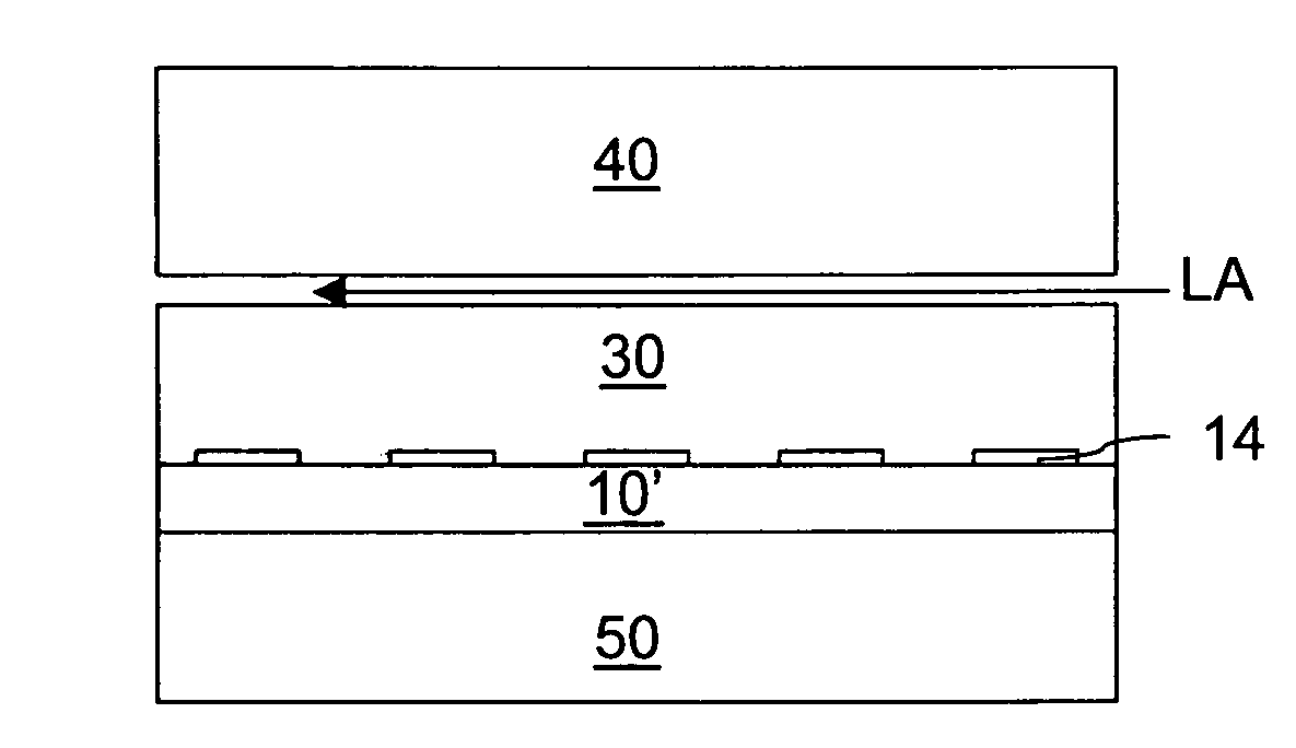
[0063]Referring to FIG. 3A, a first exemplary semiconductor structure according to a first embodiment of the present inve...


PUM


Abstract

A C4 grind tape and a laser-ablative adhesive layer are formed on a front side of a semiconductor substrate. A carrier substrate is thereafter attached to the laser-ablative adhesive layer. The back side of the semiconductor substrate is thinned by polishing or grinding, during which the carrier substrate provides mechanical support to enable thinning of the semiconductor substrate to a thickness of about 25 μm. A film frame tape is attached to the back side of the thinned semiconductor substrate and the laser-ablative adhesive layer is ablated by laser, thereby dissociating the carrier substrate from the back side of the C4 grind tape. The assembly of the film frame tape, the thinned semiconductor substrate, and the C4 grind tape is diced. The C4 grind tape is irradiated by ultraviolet light to become less adhesive, and is subsequently removed.

Description

FIELD OF THE INVENTION[0001]The present invention relates to methods of manufacturing semiconductor structures, and particularly to methods of thinning a semiconductor substrate and structures for effecting the same.BACKGROUND OF THE INVENTION[0002]Recent development in three-dimensional (3D) chip stacking technology employs thin semiconductor chips to enable vertical stacking of multiple semiconductor chips. Since a typical semiconductor substrate as manufactured in a normal semiconductor processing sequence has a thickness from about 500 μm to about 1,000 μm, formation of through-wafer vias (TWVs) that extend through the entirety of the thickness of the semiconductor substrate requires extraordinary processing sequences and high processing cost. An alternative is to thin a semiconductor substrate after the formation of semiconductor devices and interconnects on a semiconductor substrate is completed and prior to dicing the semiconductor into semiconductor chips, or “dies.” By thin...

Claims


Application Information

Patent Timeline
IPC IPC(8): H01L21/30H01L23/488
CPCH01L21/6835H01L21/6836H01L2221/68318H01L2221/68327H01L2221/6834H01L2924/09701H01L2224/16H01L2224/27436H01L2224/83191H01L2924/01057H01L2221/68381H01L2224/0554H01L2224/05568H01L2224/05573H01L2924/00014H01L2224/05599H01L2224/0555H01L2224/0556
Inventor CODDING, STEVEN R.KRYWANCZYK, TIMOTHY C.NEARY, TIMOTHY E.SPROGIS, EDMUND J.
Owner IBM CORP
Why Eureka
Try Eureka