Semiconductor laser device

a laser device and semiconductor technology, applied in semiconductor lasers, laser details, electrical equipment, etc., can solve the problems of high cost, bulky optical components, and bulky optical components of photomixing techniques

Inactive Publication Date: 2010-06-24
ELECTRONICS & TELECOMM RES INST
View PDF8 Cites 26 Cited by
  • Summary
  • Abstract
  • Description
  • Claims
  • Application Information

AI Technical Summary

Problems solved by technology

Besides, the photomixing technique needs bulky optical components such as a beam splitter or a mirror to synchronize two beams with each other and a movable and rotatable stage manipulating with accuracy below micrometer.
The bulky optical components and the stage occupy some space in the equipment employing the photomixing technique to incur high costs.

Method used


Image

  • Semiconductor laser device
  • Semiconductor laser device
  • Semiconductor laser device

Examples


Embodiment Construction

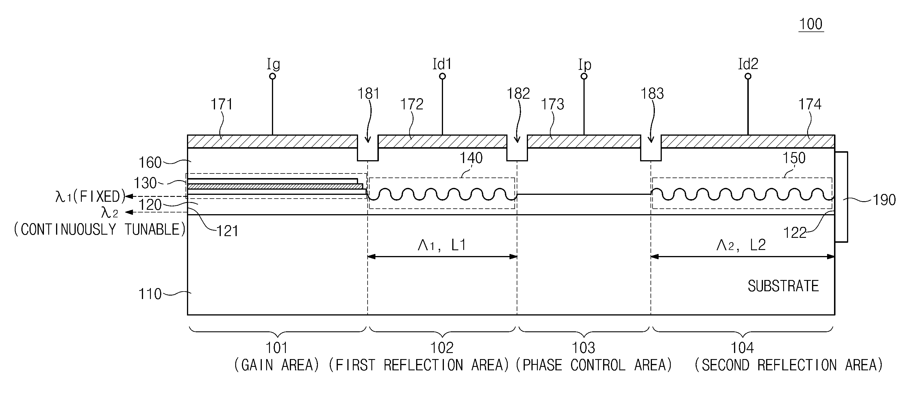
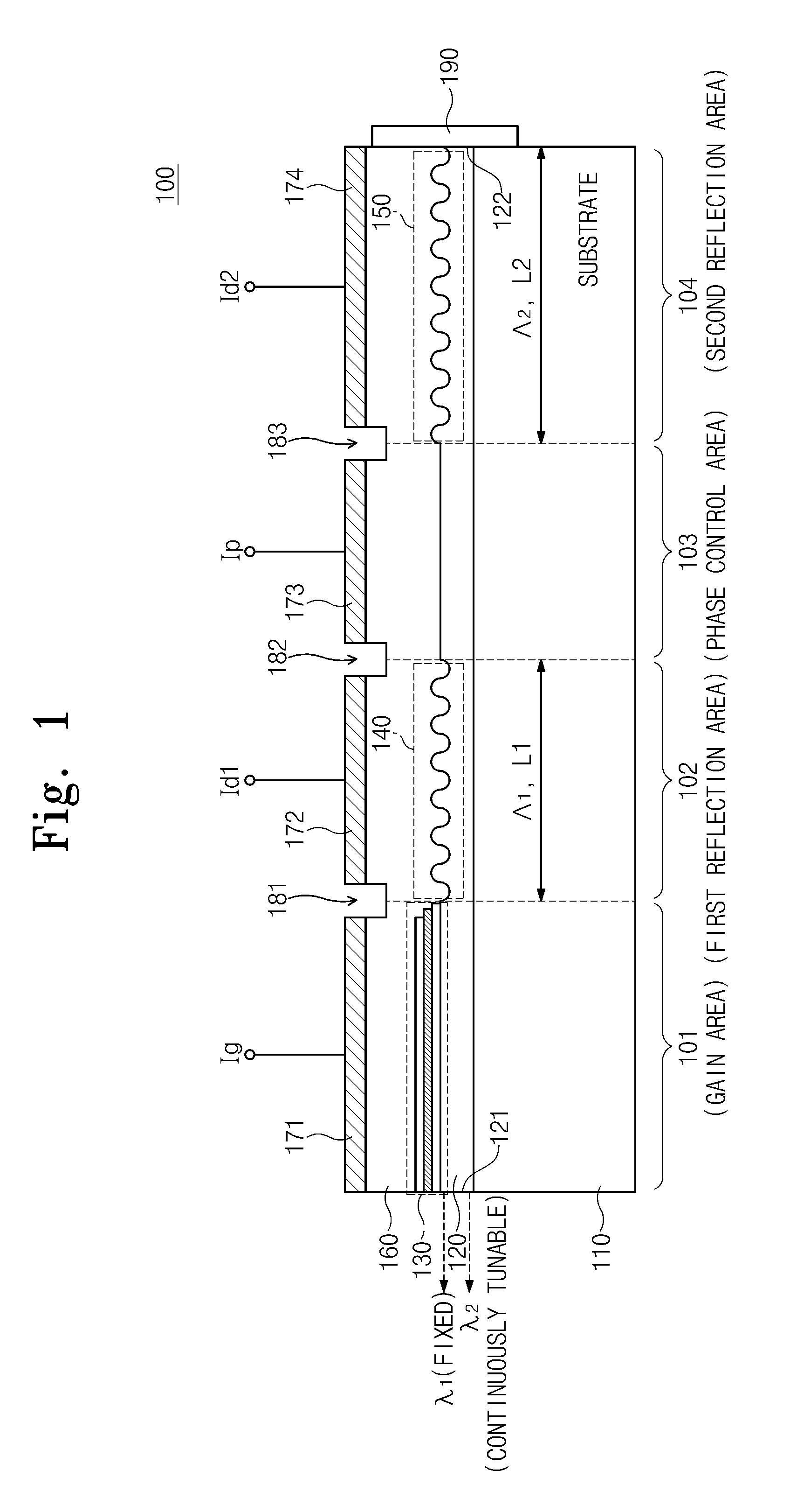
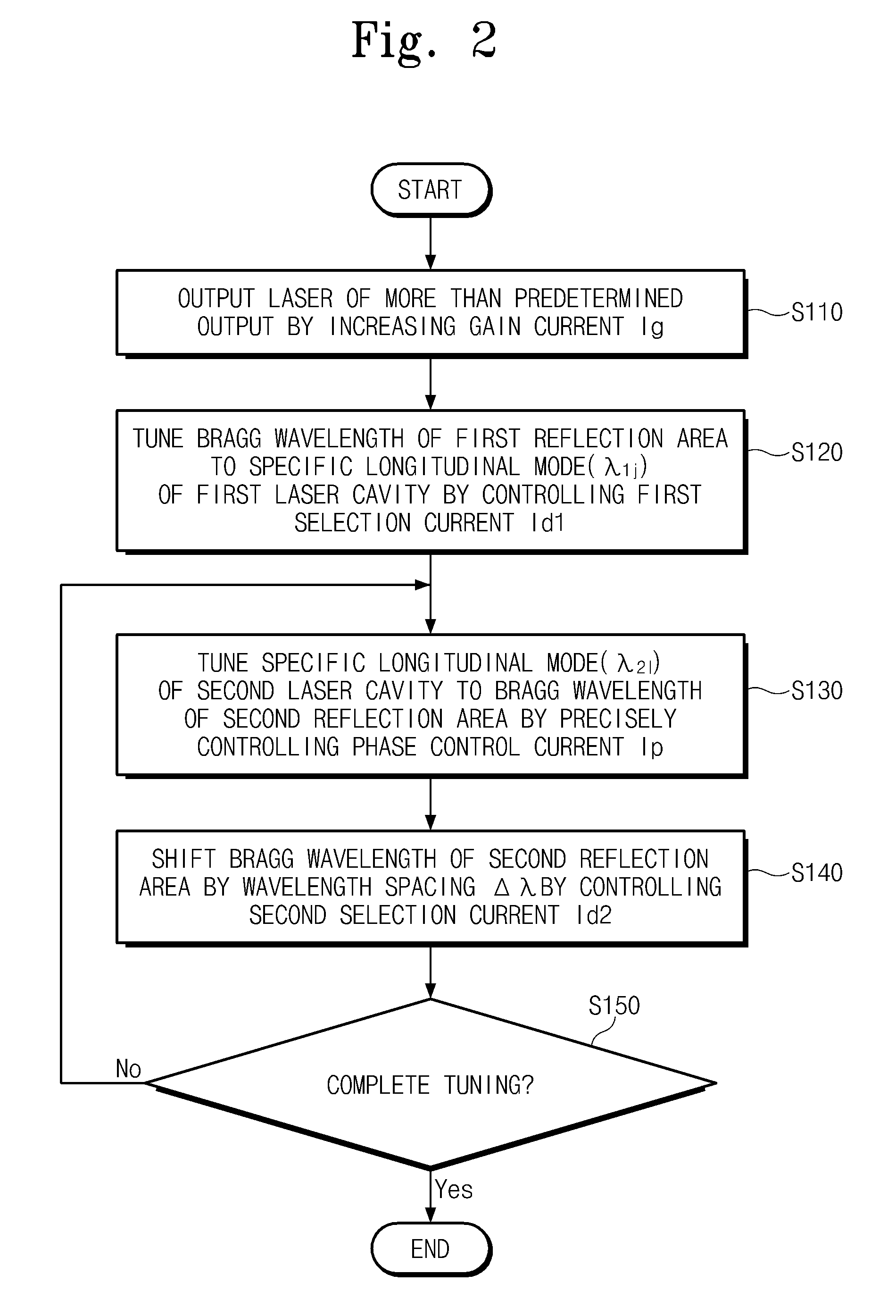
[0016]Advantages and features of the present invention and methods of accomplishing the same may be understood more readily by reference to the following detailed description of preferred embodiments and the accompanying drawings. The present invention may, however, be embodied in many different forms and should not be construed as being limited to the embodiments set forth herein. Rather, these embodiments are provided so that this disclosure will be thorough and complete and will fully convey the concept of the invention to those skilled in the art, and the present invention will only be defined by the appended claims.

[0017]It will be understood that when any layer is referred to as being “on” the other layer or substrate, it may be directly formed on the other layer or substrate or intervening layers may be present. In addition, the thickness of layer and region is exaggerated for clarity. Further, it will be understood that, although the terms first, second, third, etc. may be u...


PUM


Abstract

Provided is a semiconductor laser device including: a gain area where multi-wavelength lights are generated and gain are provided; a first reflection area where among the multi-wavelength lights, a first-wavelength light is reflected to the gain area in response to a first selection signal; a second reflection area where among the multi-wavelength lights, a second-wavelength light is reflected to the gain area; and a phase control area where a phase of the second-wavelength light is shifted in response to a phase control signal, the phase control area being disposed between the first reflection layer and the second reflection layer.

Description

CROSS-REFERENCE TO RELATED APPLICATIONS[0001]This application claims priority from Korean Patent Application No. 10-2008-0130965 filed on Dec. 22, 2008 in the Korean Intellectual Property Office, the disclosure of which is incorporated herein by reference in its entirety.BACKGROUND OF THE INVENTION[0002]1. Field of the Invention[0003]The present invention relates to semiconductor optical devices and, more particularly, to a dual-wavelength semiconductor laser device capable of continuously tuning wavelength of output light.[0004]2. Description of the Related Art[0005]As a transmittance distance increases in an optical communication system, functional optical devices have been developed for selecting specific wavelengths, for example, distributed feedback laser diode and distributed Bragg reflector laser diode, which have a narrow oscillation spectrum. Especially, optical devices have filtered wavelengths by using a diffraction grating, and various types of diffraction grating struct...

Claims


Application Information

Patent Timeline
Patent Type & Authority Applications(United States)
IPC IPC(8): H01S3/13
CPCH01S5/0623H01S2302/02H01S5/1215H01S5/06256H01S5/125
Inventor SHIN, JAE-HEONPARK, KYUNG-HYUNKIM, NAM-JELEE, CHUL-WOOKSIM, EUN-DEOKHAN, SANG-PILBAEK, YONG-SOON
Owner ELECTRONICS & TELECOMM RES INST
Why Eureka
Try Eureka