Silicon Drift X-Ray Detector

a detector and drift technology, applied in the field of x-ray detectors, can solve the problems of adversely affecting the performance of the electron microscope, increasing the background noise, and complicated magnetic fields, and achieve the effect of suppressing x-rays and reducing background nois

Active Publication Date: 2010-07-01
JEOL LTD
View PDF6 Cites 16 Cited by
  • Summary
  • Abstract
  • Description
  • Claims
  • Application Information

AI Technical Summary

Benefits of technology

[0017]It is an object of the present invention to provide a technique for reducing the background noise by suppressing X-rays which are produced secondarily by exciting the constituent elements of a cooling Peltier device with X-rays transmitted through the semiconductor device of an SDD. It is another object of the present invention to provide a technique for protecting an electron beam directed at a sample against the effect of a magnetic field produced by a cooling Peltier device in a case where an SDD is mounted in a TEM.
[0018]A first embodiment of the present invention provides a silicon drift X-ray detector for use in an energy-dispersive X-ray spectrometer installed in an X-ray analyzer that analyzes a sample by irradiating the sample with an electron beam or electromagnetic waves and spectrally detecting characteristic X-rays emanating from the sample. The X-ray detector has an X-ray detection device consisting of a solid-state semiconductor for detecting X-rays, an electrode terminal subassembly mounted to the X-ray detection device and having connector terminals for electrically connecting the X-ray detection device with an external circuit, and a Peltier device in thermal contact with the X-ray detection device via the electrode terminal subassembly to cool the X-ray detection device. A first shield made of a material consisting mainly of a chemical element having an atomic number smaller than the average atomic number of the chemical elements included in the material of the Peltier device is formed between the X-ray detection device and the Peltier device. The dose of X-rays reaching the Peltier device after being transmitted through the X-ray detection device is reduced by the first shield.

Problems solved by technology

However, if this voltage is increased excessively, it is necessary to satisfy stringent protective conditions (e.g., the inside of the container accommodating the X-ray detection device must be kept at a high vacuum).
There is the problem that the background increases because the secondary X-rays enter the X-ray detection device from the rear surface and become detected.
Another problem arises from the fact that the Peltier device is mounted close to the X-ray detection device.
If magnetic parts are present nearby, the magnetic field is complicated.
Therefore, the electron beam impinging on the sample is affected by the magnetic field produced by the Peltier device, thus adversely affecting the performance of the electron microscope.
However, this problem becomes serious when the SDD is mounted in an electron beam apparatus, such as a TEM or SEM, for analyzing a sample by irradiating the sample with an electron beam and spectrally detecting characteristic X-rays emanating from the sample.
If the EDS is a silicon drift X-ray detector (SDD), the magnetic field produced by the cooling Peltier device disturbs the magnetic field of the objective lens of the TEM, adversely affecting the electron beam.
Therefore, it is impossible to bring the EDS close to the sample to such an extent that the leaking magnetic field is affected.
Consequently, if the EDS mounted in the SEM is an SDD, the effect of the magnetic field produced from the Peltier device is weaker compared with the case where the EDS is mounted in a TEM.
That is, the problem arising from thinning of the semiconductor device of the SDD is common to both cases in which the SDD is mounted in TEM and SEM, respectively.
The problem with the magnetic field produced from the Peltier device occurs when the SDD is mounted in a TEM.

Method used


Image

  • Silicon Drift X-Ray Detector
  • Silicon Drift X-Ray Detector
  • Silicon Drift X-Ray Detector

Examples


embodiment 1

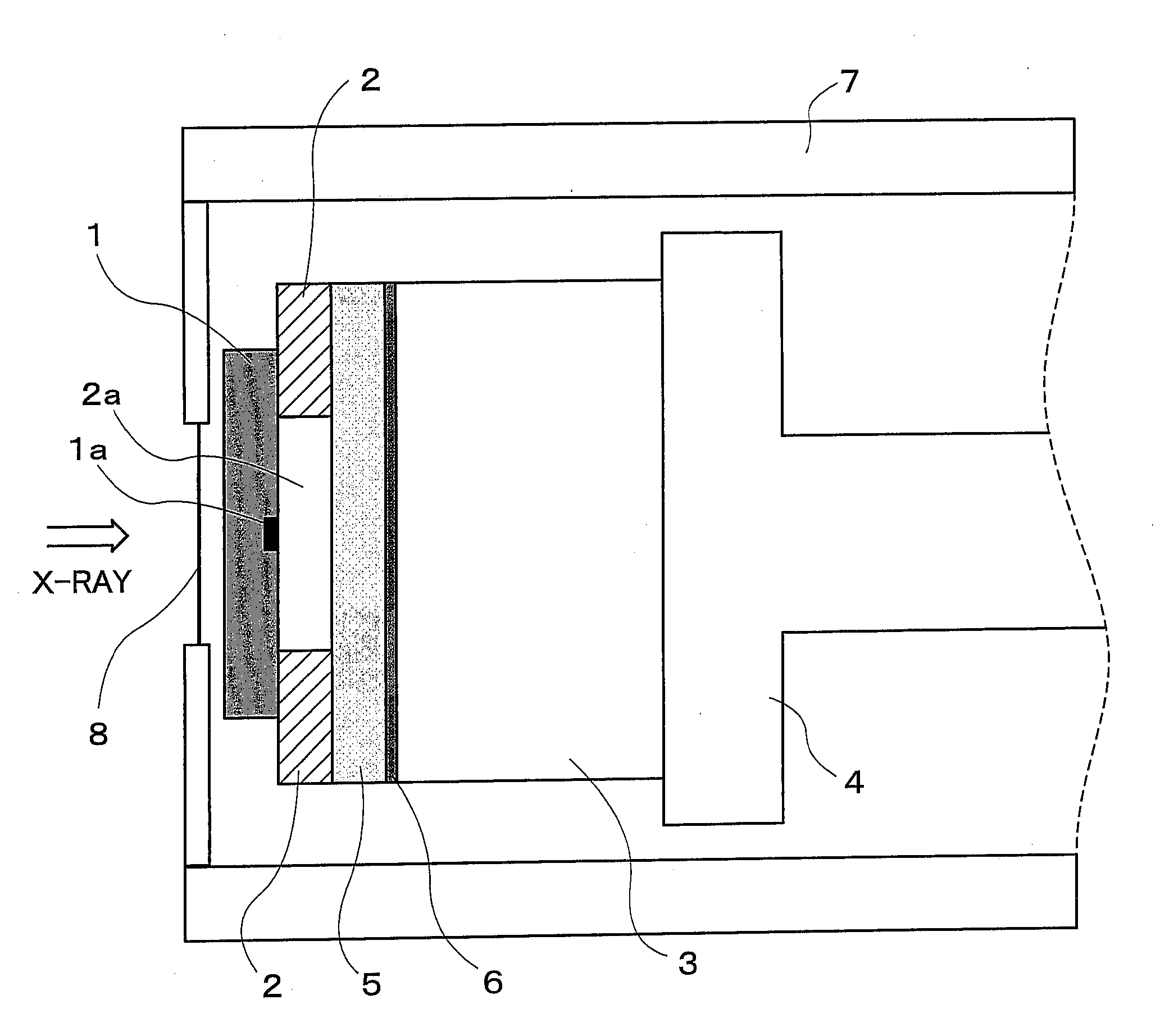
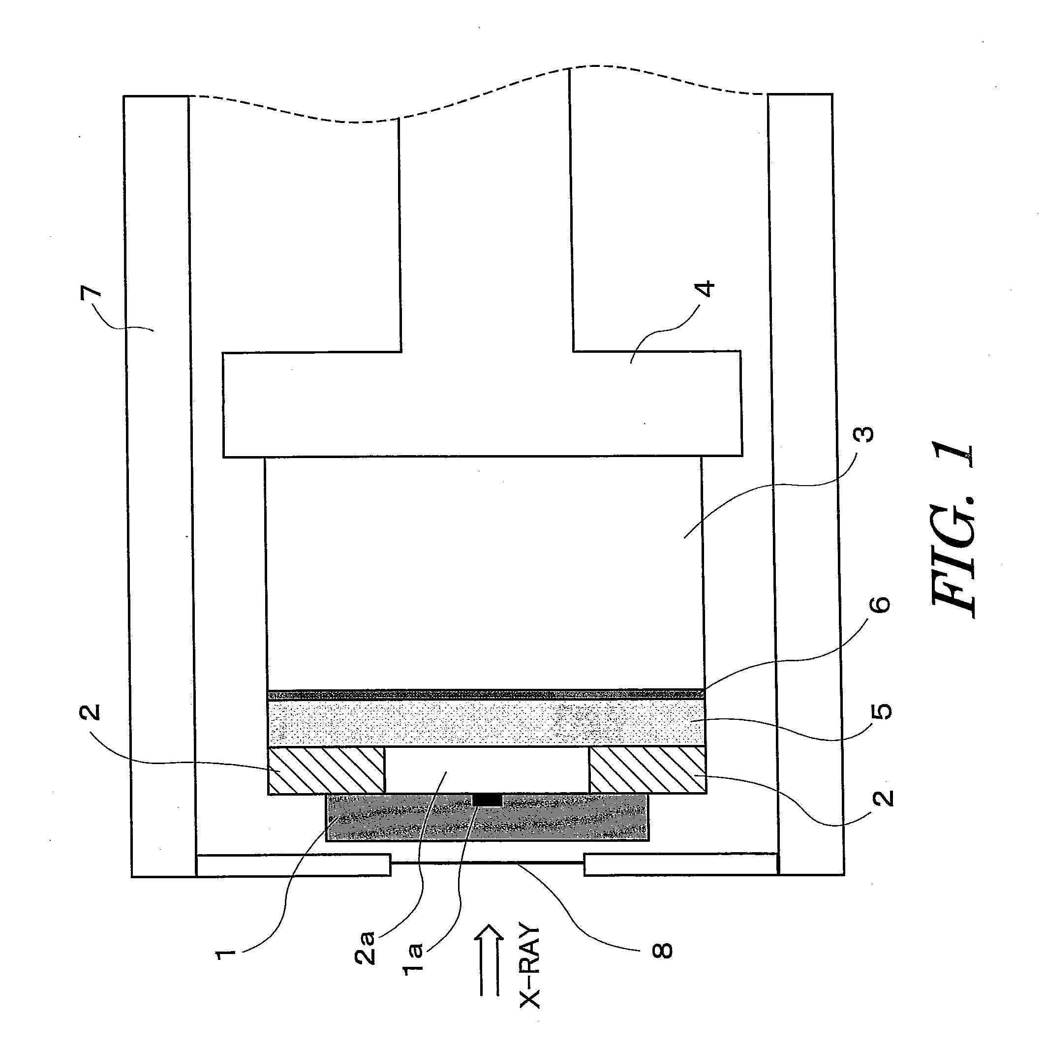
[0063]FIG. 1 is a schematic cross section of a silicon drift X-ray detector (SDD) that implements the present invention. The detector has an X-ray detection device 1 having a rear surface to which a field-effect transistor (FET) 1a is coupled. The detector further includes an electrode terminal subassembly 2 having electrical wiring for electrical connection with the X-ray detection device 1 and the FET 1a, a Peltier device 3, a rear thermal conductor 4, a first shield 5 made of a light-element material (such as boron nitride (BN) or beryllia porcelain), a second shield 6 made of a heavy-element material, such as gold leaf, a nonmagnetic outer sheath 7 for holding the cooled SDD in a vacuum environment, and an X-ray entrance window 8. The electrode terminal subassembly 2 assumes a frame-like form and has an opening 2a. The subassembly 2 is in contact with outer peripheral portions of the X-ray detection device 1 and holds it.

[0064]Since the X-ray detection device 1 is as thin as abo...

embodiment 2

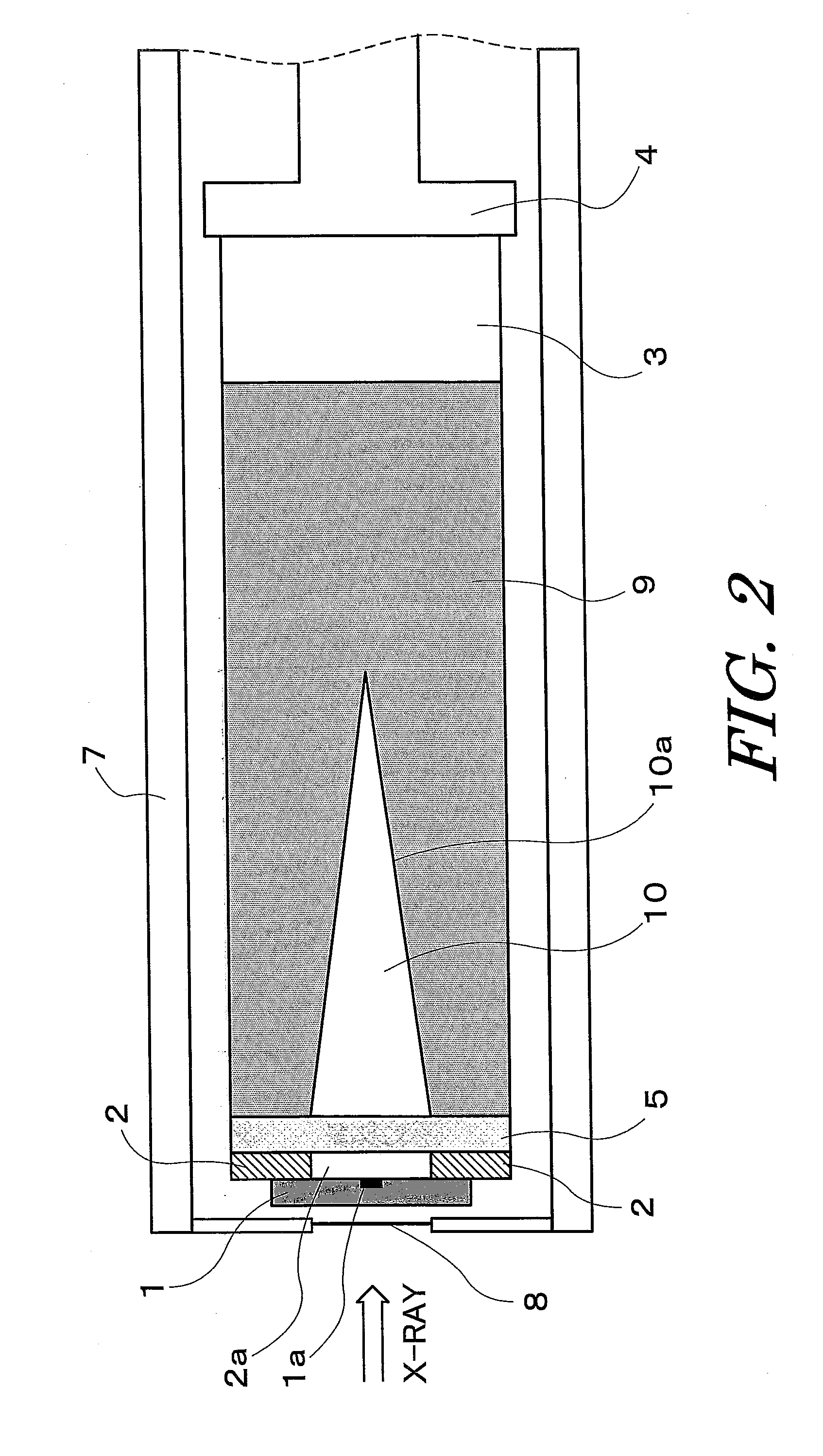
[0073]FIG. 2 is a schematic cross section of another silicon drift X-ray detector (SDD) that implements the present invention. As described previously, a large direct current flows through a Peltier device. Where the SDD of embodiment 2 is installed in a TEM, the magnetic field produced by the current flowing through the Peltier device is prevented from affecting the electron beam.

[0074]In FIG. 2, an X-ray detection device 1 has a rear surface to which a field-effect transistor (FET) 1a is coupled. An electrode terminal subassembly 2 has electrical wiring for electrical connection with the X-ray detection device 1 and the FET 1a. The SDD further includes a Peltier device 3, a rear thermal conductor 4, a first shield 5 made of a light-element material, a nonmagnetic outer sheath 7, and an X-ray entrance window 8. The electrode terminal subassembly 2 assumes a frame-like form and is provided with an opening 2a. The subassembly 2 is in contact with the outer peripheral portions of the ...


PUM


Abstract

A silicon drift detector has an X-ray detection device, an electrode terminal subassembly for electrical connection, a Peltier device, and first and second shields formed between the electrode terminal subassembly and the Peltier device. The first shield is made of a material consisting chiefly of an element having an atomic number smaller than the average atomic numbers of the elements included in the material of the Peltier device. The second shield is made of a material consisting chiefly of an element having an atomic number greater than the atomic numbers of the elements included in the material of the Peltier device

Description

BACKGROUND OF THE INVENTION[0001]1. Field of the Invention[0002]The present invention relates to an X-ray detector used to detect X-rays in an energy-dispersive X-ray spectrometer (EDS) that is mounted in a transmission electron microscope (TEM), scanning electron microscope (SEM), X-ray fluorescent analyzer (XRF), or other similar instrument and, more particularly, to a technique for reducing the background of X-rays detected by a silicon drift X-ray detector (SDD).[0003]2. Description of Related Art[0004]A PIN detector consisting of silicon (Si) doped with lithium (Li) as shown in FIG. 9 has been available as a semiconductor X-ray detector used in EDS. The semiconductor device of FIG. 9 is a PIN diode to which a reverse bias is applied. The gate of a field-effect transistor (FET) is connected with one electrode of the PIN diode. When X-rays produced from a sample impinge on the PIN semiconductor, ion pairs whose number corresponds to the energy of X-ray quanta are created. The gen...

Claims


Application Information

Patent Timeline
Patent Type & Authority Applications(United States)
IPC IPC(8): G01T1/24G01T1/36
CPCG01T1/2928H01J37/244H01J37/252H01J2237/24415H01L31/115
Inventor WATANABE, TOSHIYOSHIMIYATAKE, KOUJI
Owner JEOL LTD
Why Eureka
Try Eureka