Lateral silicon controlled rectifier structure

Active Publication Date: 2010-07-01
UNITED MICROELECTRONICS CORP
View PDF9 Cites 7 Cited by
  • Summary
  • Abstract
  • Description
  • Claims
  • Application Information

AI Technical Summary

Benefits of technology

[0009]It is one object of the invention to provide an improved silicon controlled rectifier structure for ESD protection, which is compatible wi

Problems solved by technology

Electro-static discharge (ESD) is a significant problem in integrated circuit design, especially for devices with high pin counts and circuit speeds.
It is known that the inadvertent presence of a sudden voltage spike in an integrated circuit can cause physical destruction of circuit features.
For example, ESD-induced spikes can rupture the thin gate oxide of a field effect tran

Method used


Image

  • Lateral silicon controlled rectifier structure
  • Lateral silicon controlled rectifier structure
  • Lateral silicon controlled rectifier structure

Examples


Example

[0018]The present invention has been particularly shown and described with respect to certain embodiments and specific features thereof. The embodiments set forth hereinbelow are to be taken as illustrative rather than limiting. It should be readily apparent to those of ordinary skill in the art that various changes and modifications in form and detail may be made without departing from the spirit and scope of the invention.

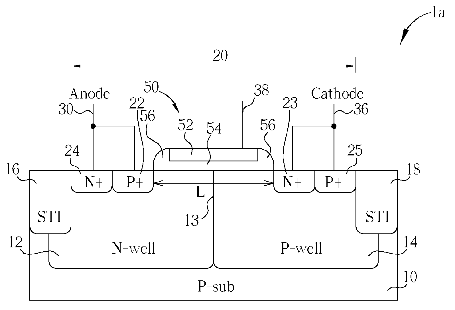
[0019]The present invention pertains to an improved silicon controlled rectifier (SCR) structure for ESD protection, which is compatible with current CMOS processes, which has lower threshold trigger voltages and improved efficiency, and which occupies relatively smaller chip areas.

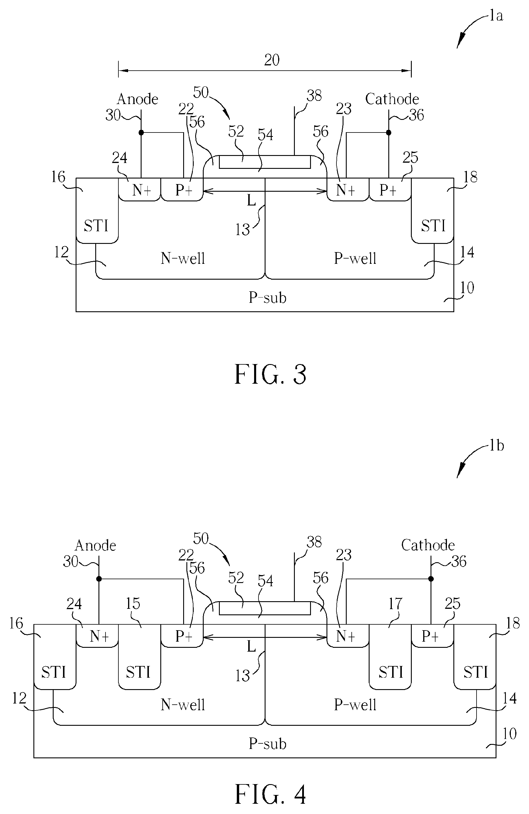
[0020]FIG. 3 is a schematic, cross-sectional view of an improved lateral silicon controlled rectifier (LSCR) structure 1a in accordance with one preferred embodiment of the present invention. As shown in FIG. 3, the LSCR structure 1a is fabricated within an active area 20 that is defin...


PUM


Abstract

A lateral silicon controlled rectifier structure includes a P-type substrate; an N-well region in the P-type substrate; a first P+ doped region in the N-well region and being connected to an anode; a P-well region in the P-type substrate and bordering upon the N-well region; a first N+ doped region formed in the P-well region and separated from the first P+ doped region by a spacing distance, the first N+ doped region being connected to a cathode; and a gate structure overlying a portion of the P-type substrate between the first P+ doped region and the first N+ doped region.

Description

BACKGROUND OF THE INVENTION [0001]1. Field of the Invention[0002]This invention relates in general to electronic circuits, and more particularly, to lateral silicon controlled rectifier (LSCR) structures for electro-static discharge (ESD) protection.[0003]2. Description of the Prior Art[0004]Electro-static discharge (ESD) is a significant problem in integrated circuit design, especially for devices with high pin counts and circuit speeds. ESD refers to the phenomena wherein a high-energy electrical discharge of current is produced at the input and / or output nodes of an integrated circuit (IC) device as a consequence of static charge build-up on the IC package. The static charge build up can result from handling of the IC device by a human body or from handling by IC device manufacturing equipments. It is known that the inadvertent presence of a sudden voltage spike in an integrated circuit can cause physical destruction of circuit features. For example, ESD-induced spikes can ruptur...

Claims


Application Information

Patent Timeline
IPC IPC(8): H01L29/735
CPCH01L27/0259H01L29/0653H01L29/7436
Inventor LIN, TA-CHENGWU, TE-CHANG
Owner UNITED MICROELECTRONICS CORP
Why Eureka
Try Eureka