Hall Element and Magnetic Sensor

a technology of magnetic sensor and hall element, which is applied in the field of hall element and magnetic sensor, can solve the problems of s/n ratio, preventing the practical use of such a monolithic azimuth sensor, and complex construction, and achieves improved s/n ratio per current, high breakdown voltage, and high sensitivity.

Active Publication Date: 2010-07-01
ASAHI KASEI ELECTRONICS CO LTD
View PDF4 Cites 34 Cited by
  • Summary
  • Abstract
  • Description
  • Claims
  • Application Information

AI Technical Summary

Benefits of technology

[0016]According to the present invention, the p-type impurity region is located in a surface of the n-type impurity region, while the n-type impurity region is surrounded by the p-type substrate region of the p-type semiconductor substrate layer. By so limiting the low-concentration n-well within a suitable range, the present invention achieves the effect of realizing a Hall element which has a high sensitivity and contributes to an improvement in S / N ratio per current, as well as a Hall element having a high breakdown voltage and high reliability.
[0017]Also, since the magnetic sensing part is formed so as to be surrounded by the p-type substrate region, the present invention achieves not only the effect of realizing the Hall element having a high breakdown voltage and high reliability but also the effect of becoming less susceptible to noise caused by coupling by virtue of a reduction in the junction capacitance around the magnetic sensing part.

Problems solved by technology

For this reason, a signal processing chip and the azimuth sensor have been required to be placed in separate arrangements, thus making the construction complicated.
Though it has been desired to develop an Si monolithic azimuth sensor, the insufficient S / N ratio due to a low sensitivity of an Si Hall element has precluded the practical use of such an Si monolithic azimuth sensor.

Method used


Image

  • Hall Element and Magnetic Sensor
  • Hall Element and Magnetic Sensor
  • Hall Element and Magnetic Sensor

Examples


example 1

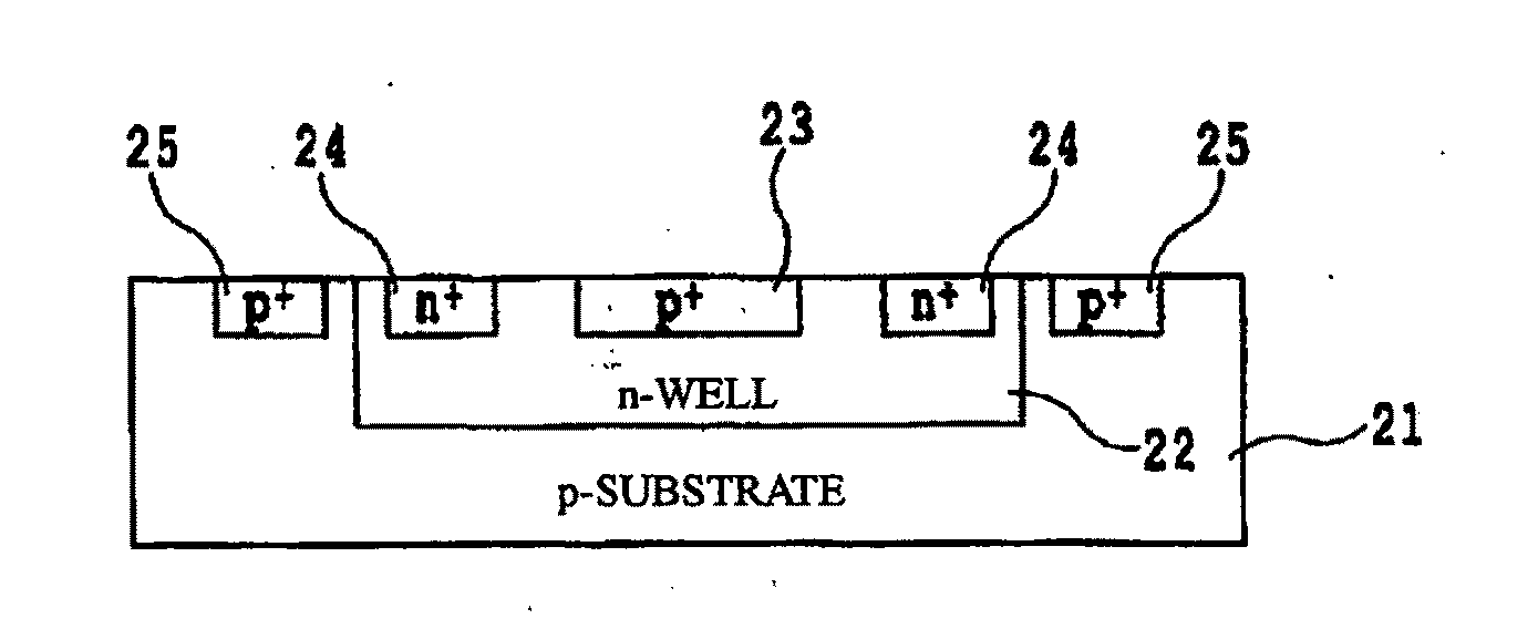
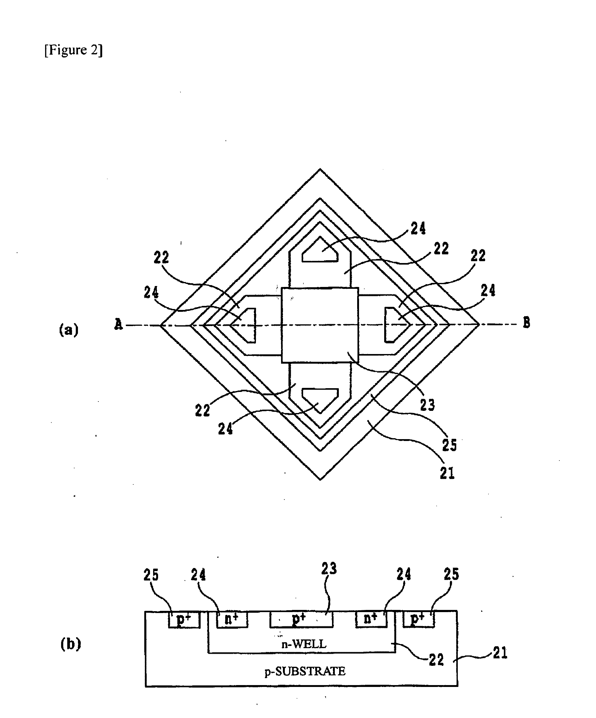
[0062]FIGS. 2(a) and 2(b) are each a schematic view for illustrating Example 1 of a Hall element according to the present invention; FIG. 2(a) is a top plan view and FIG. 2(b) is a sectional view taken on line A-B of FIG. 2(a). Reference numeral 21 designates a p-type semiconductor substrate layer, 21a designates a p-type substrate region, 22 designates an n-type impurity region (n-well), 23 designates a p-type impurity region (p+ diffusion layer), 24 designates an n-type region (n+ diffusion layer), 25 designates a p-type region (p+ diffusion layer), 26 designates a magnetic sensing part, and 27 designates an electrode.

[0063]The Hall element of the present invention includes the p-type semiconductor substrate layer 21 composed of p-type silicon, and the n-type impurity region 22 located in a surface of the p-type semiconductor substrate layer 21. The n-type impurity region 22 functions as the magnetic sensing part 26.

[0064]The p-type impurity region 23 is located in a surface of th...

example 2

[0078]FIG. 7 is a schematic sectional view taken on line A-B of FIG. 2(a) for illustrating Example 2 of a Hall element according to the present invention. In FIG. 7, reference numeral 28 designates a depletion layer, and reference characters C1, C2 and C3 designate junction capacitances. Other reference numerals are each the same as used in FIG. 2(b).

[0079]In Example 2, a wide region of the depletion layer 28 is provided at the interface between the n-type impurity region 22 and the p-type semiconductor substrate layer 21. That is, this arrangement allows a depletion layer width to increase at the interface between the low-concentration p-type semiconductor substrate layer 21 and the low-concentration n-well 22. For this reason, the junction capacitances C1, C2 and C3 are reduced, so that coupling noise from the p-type semiconductor layer 21 is reduced, thus resulting in an improved S / N ratio. Further, an improvement in breakdown voltage ensures high reliability and, hence, it is po...


PUM


Abstract

A Hall element is provided which has a high sensitivity and contributes to an improvement in S/N ratio per current by using a low-concentration n-well within a suitable range. The Hall element includes a p-type semiconductor substrate layer 21 of p-type silicon, and an n-type impurity region 22 located in a surface of the p-type semiconductor substrate layer 21, the n-type impurity region 22 functioning as a magnetic sensing part 26. A p-type impurity region 23 is located in a surface of the n-type impurity region 22, and n-type regions 24 are located laterally of the p-type impurity region 23. A p-type substrate region 21a having a resistivity equal to that of the p-type semiconductor substrate layer 21 is located to extend around the n-type impurity region 22. An impurity concentration N in the n-type impurity region 22 functioning as the magnetic sensing part 26 is preferably from 1×10¹⁶ to 3×10¹⁶ (atoms/cm3), and a distribution depth D of the impurity concentration is preferably from 3.0 μm to 5.0 μm.

Description

TECHNICAL FIELD[0001]The present invention relates to a Hall element and a magnetic sensor and, more specifically, to a Hall element having an n-type impurity region located in a surface of a p-type semiconductor substrate layer composed of p-type silicon, the n-type impurity region functioning as a magnetic sensing part, as well as a magnetic sensor using the Hall element. Particularly, the Hall element and the magnetic sensor are for use in an azimuth sensor.BACKGROUND ART[0002]Conventionally, an azimuth sensor which detects the earth magnetism to determine an azimuth has employed a Hall element having a high sensitivity for detecting the weak earth magnetism. Hall elements of this type include a conventionally well-known Hall element adapted to detect a magnetic field component perpendicular to a substrate surface (i.e., chip face), and a vertical Hall device adapted to detect a magnetic field component horizontal to a substrate surface (i.e., chip face).[0003]FIG. 1 is a schemat...

Claims


Application Information

Patent Timeline
Patent Type & Authority Applications(United States)
IPC IPC(8): H01L43/06
CPCG01R33/07G01R33/075H01L43/065H10N52/101
Inventor NAMAI, TAKAYUKIKAKUTA, KATSUMI
Owner ASAHI KASEI ELECTRONICS CO LTD
Why Eureka
Try Eureka