

Semiconductor device
- Summary
- Abstract
- Description
- Claims
- Application Information
AI Technical Summary
Benefits of technology
Problems solved by technology
Method used
Image

Examples
Embodiment Construction
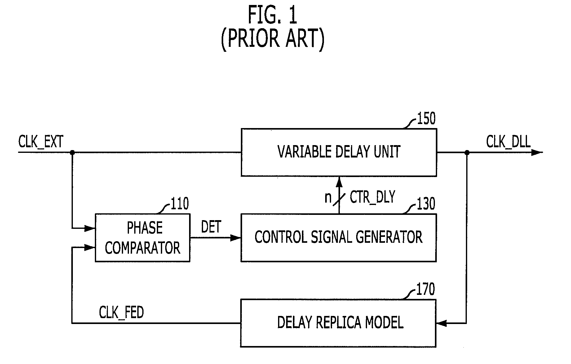
[0052]Hereinafter, a register controlled Delay Locked Loop (DLL) circuit in accordance with the present invention will be described in detail with reference to the accompanying drawings.
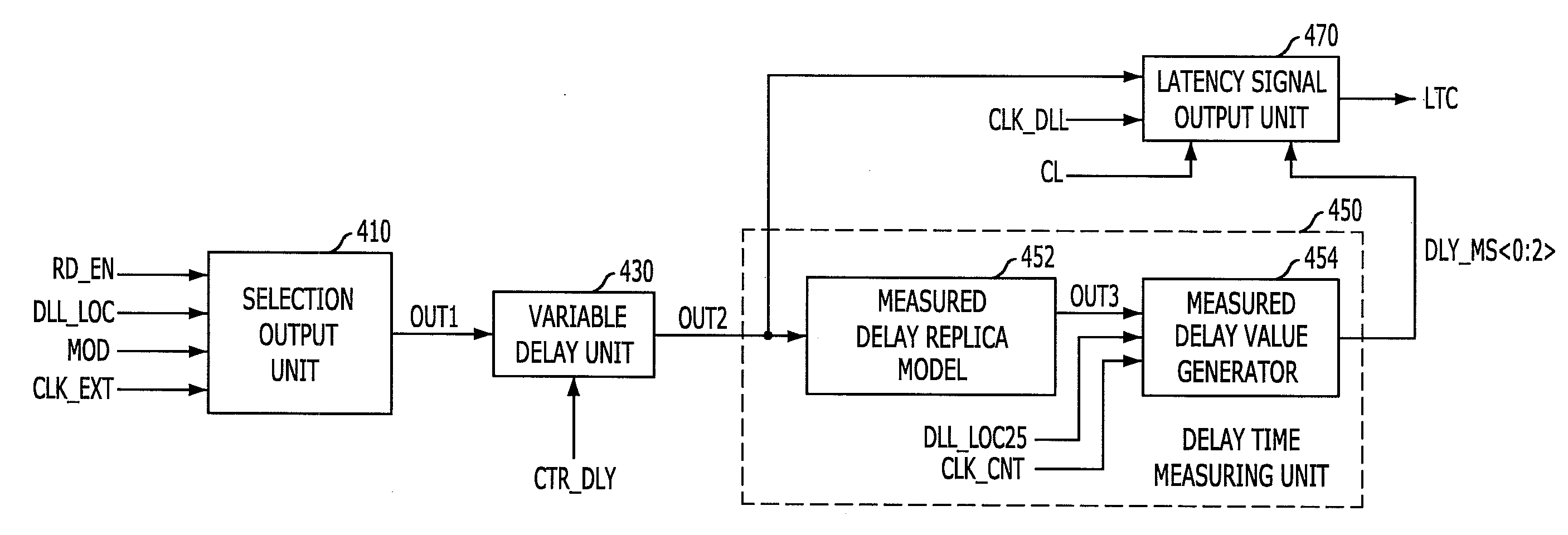
[0053]FIG. 4 is a block diagram illustrating a latency signal generating circuit of a semiconductor device in accordance with an embodiment of the present invention.
[0054]Referring to FIG. 4, the latency signal generating circuit according to the present embodiment calculates a measured delay value DLY_MS representing a delay amount between a reference clock signal CLK_REF (see FIG. 13) and a feedback clock signal CLK_FED (see FIG. 13) in response to a locking completion signal DLL_LOC synchronized with an external clock signal CLK_EXT and generates a latency signal LTC by synchronizing a read command signal RD_EN15, which was synchronized with an external clock signal CLK_EXT, with the DLL clock signal CLK_DLL. The latency signal generating circuit according to the present embodiment includes a sele...
PUM
 Abstract
Description
Claims
Application Information