
Eureka
For R&D, Eureka makes reading and utilizing patents & technical documents easy.
Eureka AIR
Designed for self-driven R&D workflows. Generate viable solutions, solve complex R&D challenges, empower your innovation with AI.

Eureka Materials
Designed for material experts only. Revolutionize your material R&D, from search, analyze, to developing new materials.

TechResearch
Generate reliable direction feasibility study reports for your R&D in just a few steps.

TechSeek
Discover and master advanced knowledge NOW. Basics, ideas, possibilities, all at once.

TechMind
As an expert in R&D Theories, TechMind can generates customized viable solutions instantly.

TechRisk
Analyze your overall solution with one click, know your potential R&D risks in advance.

TechMonitor
Get weekly tech updates, stay abreast of the latest tech innovations and key insights.
Semiconductor device
- Summary
- Abstract
- Description
- Claims
- Application Information
AI Technical Summary
Benefits of technology
Problems solved by technology
Method used
Image

Examples
first embodiment
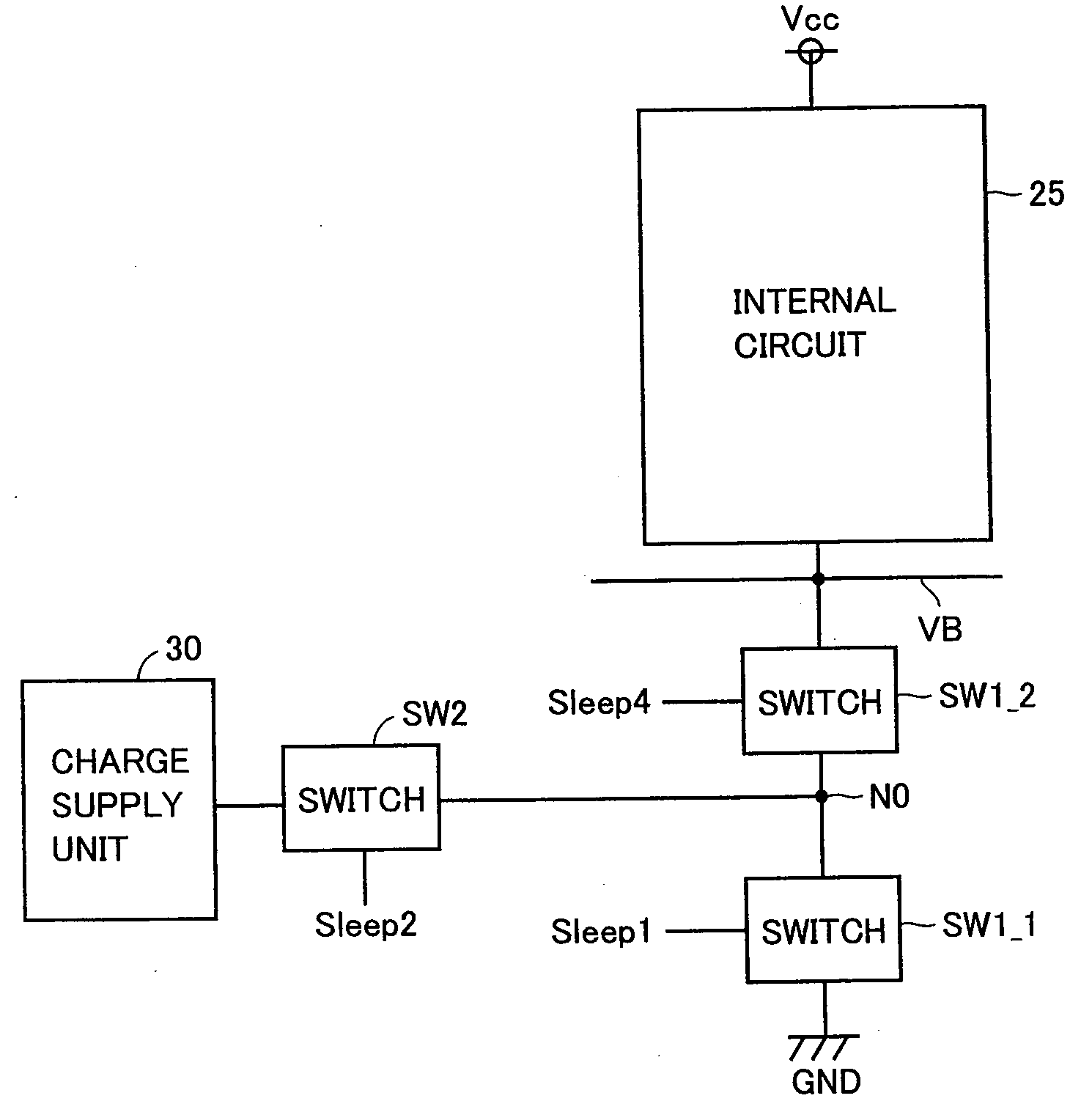
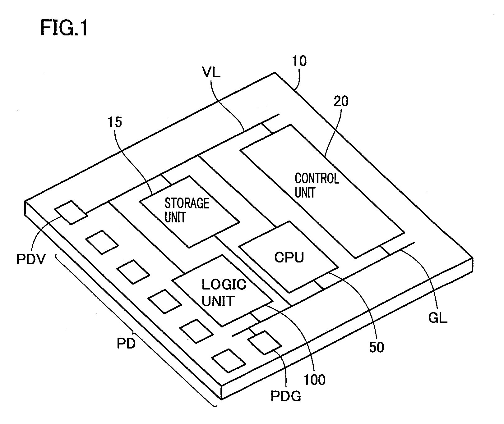
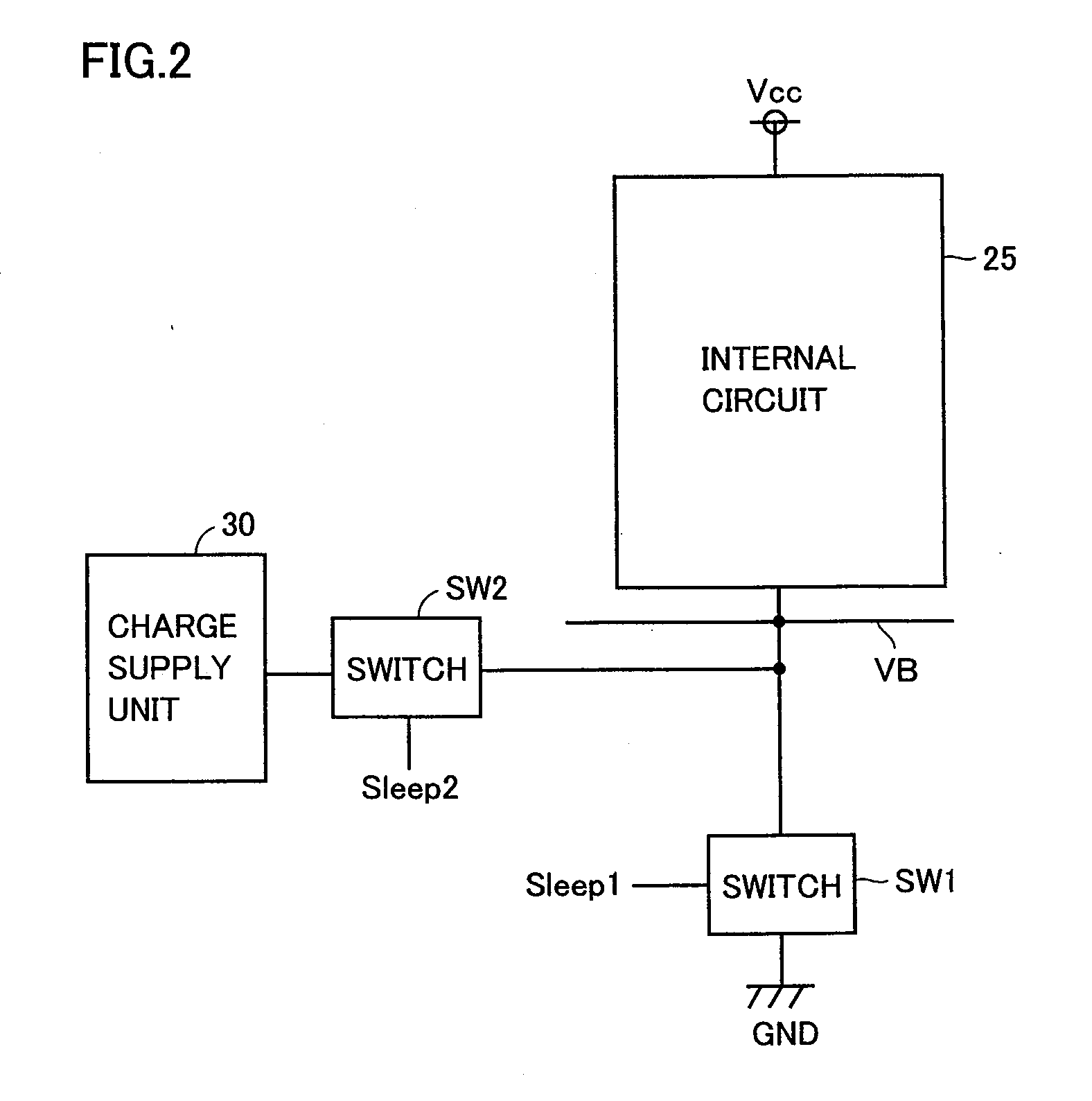
[0077]FIG. 1 schematically shows a structure of a chip 10 according to a first embodiment of the invention.
[0078]Referring to FIG. 1, a chip 10 according to the embodiment of the invention includes a CPU 50 for controlling a whole circuit, a storage unit 15 having a memory for storing information, a control unit 20 that is a peripheral circuit for producing a clock signal or control signals based on commands from CPU 50 and a logic unit 100 for executing various arithmetic operations.
[0079]Chip 10 is provided at its peripheral region with pads, which are a power supply pad PDV supplying a power supply voltage Vcc, a ground pad PDG supplying a ground voltage GND and a pad PD externally receiving a command signal and the like in this example.
[0080]Ground pad PDG is electrically coupled to a ground line GL for supplying a ground voltage of the circuit, and is supplied with ground voltage GND. Power supply pad PDV is electrically coupled to a power supply line VL for supplying power sup...
second embodiment
[0253]In a second embodiment of the invention described below, a switch does not operate at the time of switching of the operation mode, but operates during the operation mode.
[0254]An example of the second embodiment will be described in connection with a low power consumption operation mode of the SRAM memory cell.
[0255]FIG. 23 is a schematic structural diagram illustrating a part of a storage unit 15 according to a second embodiment of the invention.
[0256]Referring to FIG. 23, storage unit 15 according to the second embodiment of the invention includes a memory array MA including MC arranged in rows and columns, a row decoder 62 selecting a row of memory cells MC, a column decoder 66 selecting a column of memory cells MC and a control circuit 63 for controlling a circuit block of the row decoder, column decoder and others, and also includes a data line IO and a complementary data line / IO used for reading and writing data. In this example, control circuit 63 receives a clock CLK ...
third embodiment
[0336]The embodiments have been described in connection with examples that reduce power consumption in one chip. However, the chip is not restricted to one in number. For example, the similar configuration can be applied to semiconductor devices, e.g., of an SIO (System In Package) structure in which a plurality of chips are included in one package.
[0337]FIG. 32 illustrates a semiconductor device of the SIO structure.
[0338]Referring to FIG. 32, chip 10 and another chip 10# are arranged in one package. The SIP structure can reduce a circuit board and can achieve fast data transfer. In this example, a pad PDa on chip 10 is connected by wire bonding to a pad PDb on chip 10#.
[0339]FIG. 33 illustrates an MTCMOS circuit according to the third embodiment of the invention. The following description will be given, by way of example, in connection with the structure in FIG. 3(a) and particularly in connection with logic circuit group L1 included in logic unit 100 on the chip 10 side and logic...
PUM
 Abstract
Description
Claims
Application Information
 - R&D Engineer
- R&D Manager
- IP Professional
- Industry Leading Data Capabilities
- Powerful AI technology
- Patent DNA Extraction
Browse by: Latest US Patents, China's latest patents, Technical Efficacy Thesaurus, Application Domain, Technology Topic, Popular Technical Reports.
© 2024 PatSnap. All rights reserved.Legal|Privacy policy|Modern Slavery Act Transparency Statement|Sitemap|About US| Contact US: help@patsnap.com