Compact scanning electron microscope

a scanning electron microscope and compact technology, applied in the field of electron microscopes, can solve the problems of high cost of sem devices, high equipment cost, and high equipment cost, and achieve the effects of small dimensions, low cost, and easy us

Active Publication Date: 2010-07-08
FEI CO
View PDF57 Cites 30 Cited by
  • Summary
  • Abstract
  • Description
  • Claims
  • Application Information

AI Technical Summary

Benefits of technology

[0007]An object of the invention is to provide a scanning electron microscope that is inexpensive, easy to use, and can be of sufficiently small dimensions that it can be placed, for example, atop a classroom table.

Problems solved by technology

Electron microscopes are typically large, complex, and expensive instruments that require skilled technicians to operate them.
SEM devices typically cost well over $100,000 and require special facilities, including dedicated electrical wiring and venting of the vacuum pump outside of the operator area.
Further, it can be difficult in a high magnification image such as that of an SEM for a user to determine where on the sample an image is being obtained and to understand the relationship between that image and the rest of the sample.
The cost of electron microscopes and the sophistication required to operate them have limited their use to research and industry that can afford the cost and provide the expertise to operate.
After a sample is inserted, it typically takes a relatively long period of time for air in the chamber to be evacuated, so that a user must wait before an image is available.
This delay makes use of an SEM impractical in many applications.

Method used


Image

  • Compact scanning electron microscope
  • Compact scanning electron microscope
  • Compact scanning electron microscope

Examples


Embodiment Construction

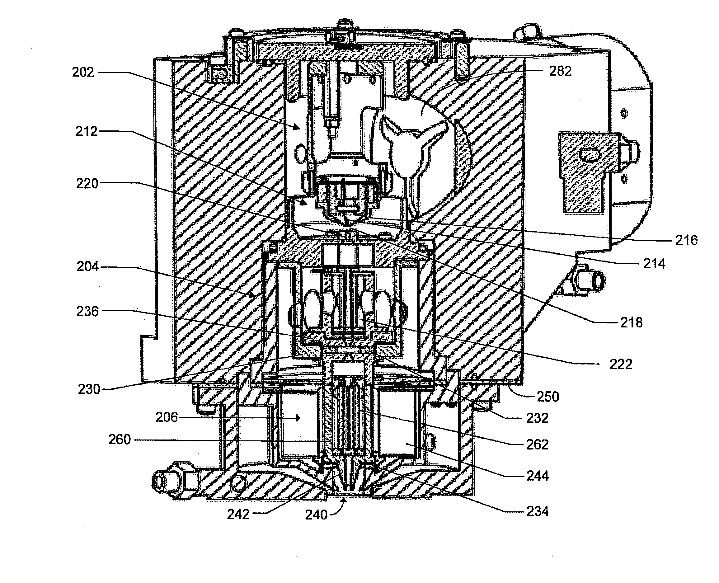
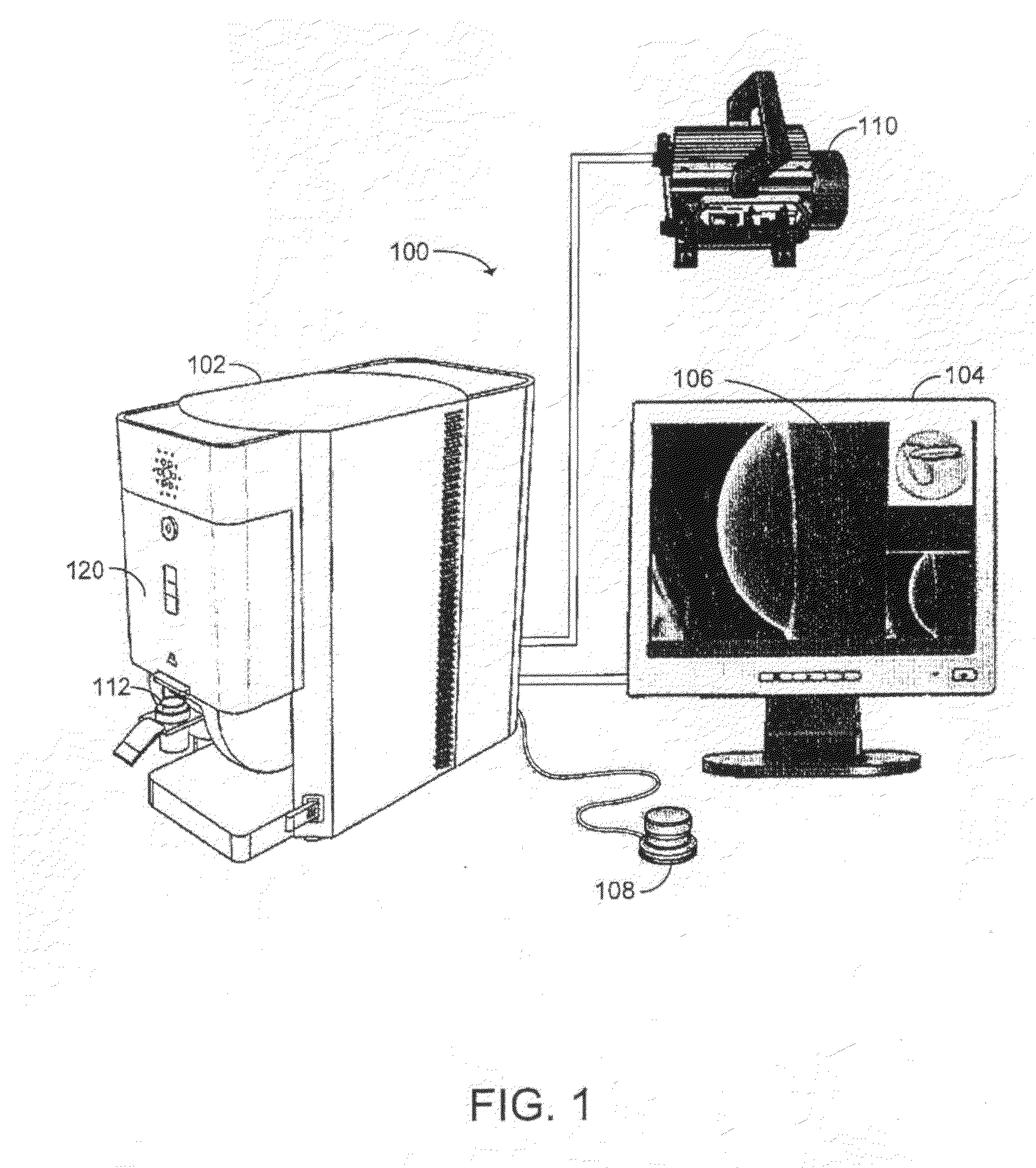
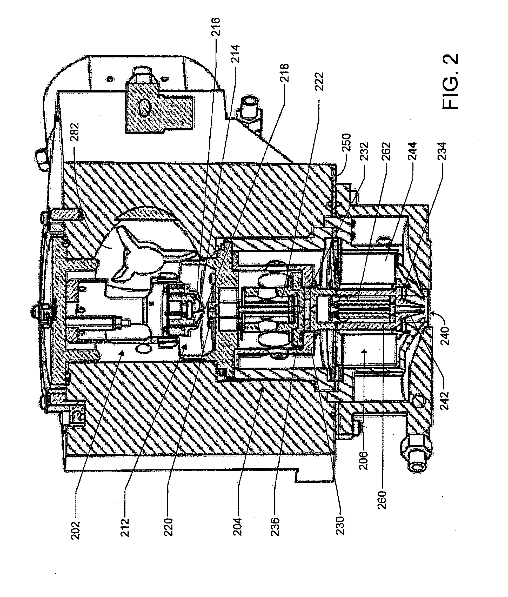
[0027]FIG. 1 shows the exterior of a preferred embodiment of an electron microscope system 100 of the present invention that includes SEM assembly 102, a display monitor 104, preferably incorporating a touch screen 106 for accepting user input, an rotary user input device 108, and an external pre-vacuum pump 110, such as a diaphragm pump. A sample holder 112 holds the sample to be viewed and is inserted into SEM assembly 102.

[0028]Electron microscope system 100 require no special facilities installation, that is, a preferred embodiment can operate on conventional power, that is, by plugging into a wall socket, and the vacuum system does not require venting to outside of the operator area. SEM assembly 102 does not require special vibration damping mounting. SEM assembly 102 is literally a “table-top SEM,” that can be set on any sturdy work surface and plugged into the wall. Electron microscope system 100 is therefore suitable for use in classroom or even in homes. Some embodiments c...


PUM


Abstract

A compact electron microscope uses a removable sample holder having walls that form a part of the vacuum region in which the sample resides. By using the removable sample holder to contain the vacuum, the volume of air requiring evacuation before imaging is greatly reduced and the microscope can be evacuated rapidly. In a preferred embodiment, a sliding vacuum seal allows the sample holder to be positioned under the electron column, and the sample holder is first passed under a vacuum buffer to remove air in the sample holder.

Description

[0001]The present application claims priority from International Application PCT / US2007 / 070655, filed Jun. 7, 2007, and from U.S. Provisional Application 60 / 811,621, filed Jun. 7, 2006, which are hereby incorporated by reference.TECHNICAL FIELD OF THE INVENTION[0002]The present invention relates to electron microscopes.BACKGROUND OF THE INVENTION[0003]Electron microscopy provides significant advantages over optical microscopy, such as higher resolution and greater depth of focus. In a scanning electron microscope (SEM) a primary electron beam is focused to a fine spot that scans the surface to be observed. Secondary electrons are emitted from the surface as it is impacted by the primary beam and some electrons from the primary beam are backscattered. The secondary or backscattered electrons are detected and an image is formed, with the brightness at each point of the image being determined by the number of electrons detected when the beam impacts a corresponding spot on the surface....

Claims


Application Information

Patent Timeline
Patent Type & Authority Applications(United States)
IPC IPC(8): H01J37/28
CPCH01J37/16H01J37/18H01J37/20H01J37/226H01J37/244H01J37/28H01J37/21H01J2237/162H01J2237/1825H01J2237/188H01J2237/2003H01J2237/2006H01J37/185H01J2237/1405H01J37/302H01J37/26H01J37/261
Inventor BIERHOFF, MART PETRUS MARIABUIJSSE, BARTKOOIJMAN, CORNELIS SANDERVAN LEEUWEN, HUGOTAPPEL, HENDRIK GEZINUSSANFORD, COLIN AUGUSTSTOKS, SANDER RICHARD MARIEBERGER, STEVENBORMANS, BEN JACOBUS MARIEDRIESSEN, KOEN ARNOLDUS WILHELMUSPERSOON, JOHANNES ANTONIUS HENDRICUS W. G.
Owner FEI CO
Why Eureka
Try Eureka