
Eureka
For R&D, Eureka makes reading and utilizing patents & technical documents easy.
Eureka AIR
Designed for self-driven R&D workflows. Generate viable solutions, solve complex R&D challenges, empower your innovation with AI.

Eureka Materials
Designed for material experts only. Revolutionize your material R&D, from search, analyze, to developing new materials.

TechResearch
Generate reliable direction feasibility study reports for your R&D in just a few steps.

TechSeek
Discover and master advanced knowledge NOW. Basics, ideas, possibilities, all at once.

TechMind
As an expert in R&D Theories, TechMind can generates customized viable solutions instantly.

TechRisk
Analyze your overall solution with one click, know your potential R&D risks in advance.

TechMonitor
Get weekly tech updates, stay abreast of the latest tech innovations and key insights.
Substrate processing method
- Summary
- Abstract
- Description
- Claims
- Application Information
AI Technical Summary
Benefits of technology
Problems solved by technology
Method used
Image

Examples
first embodiment
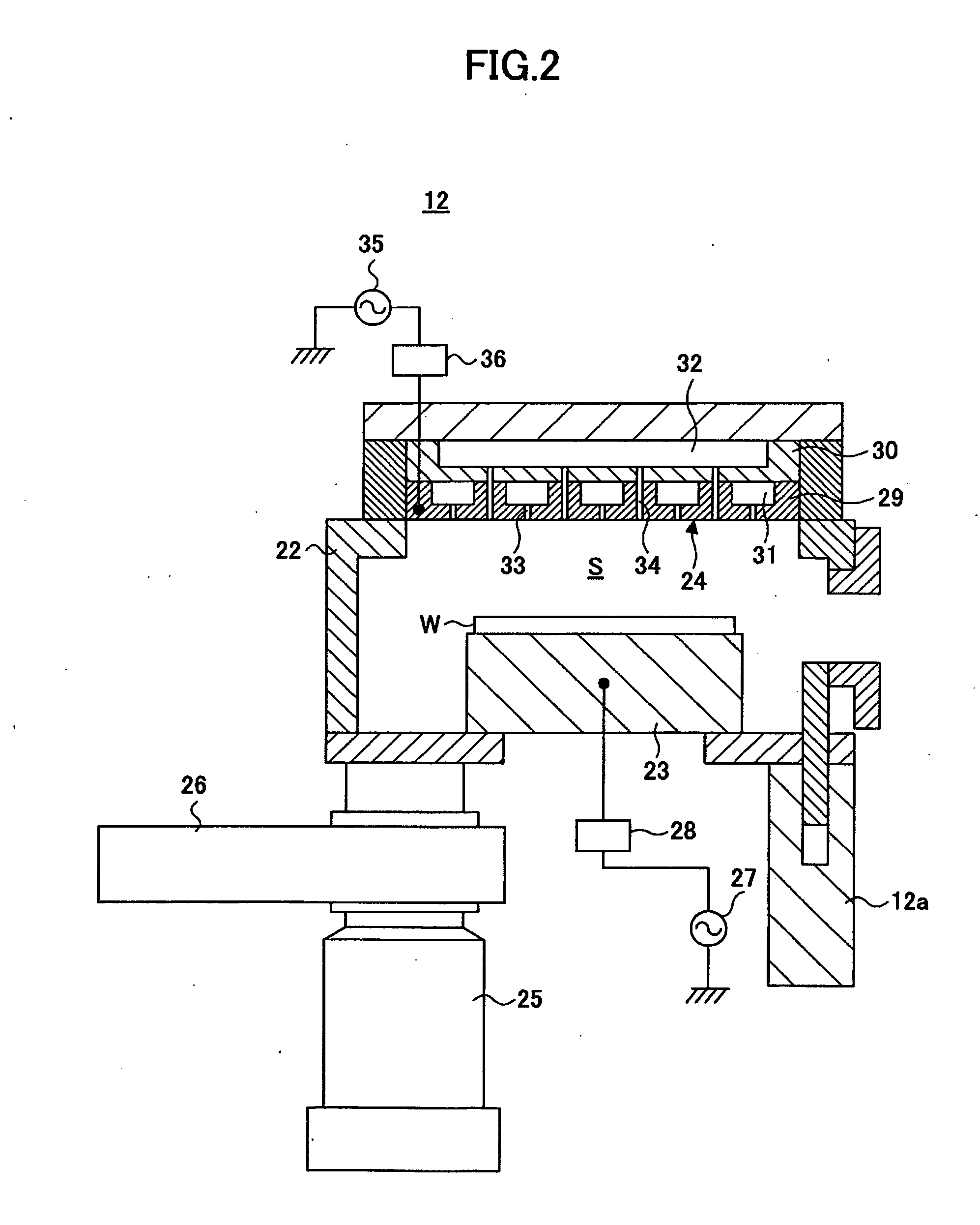
[0028]First, a description is made on a substrate processing system which is configured to perform a substrate processing method of the invention. This substrate processing system includes plural process modules configured to apply an etching treatment or an asking treatment by applying plasma to a semiconductor wafer W (hereinafter simply called a “wafer W”) serving as a substrate.
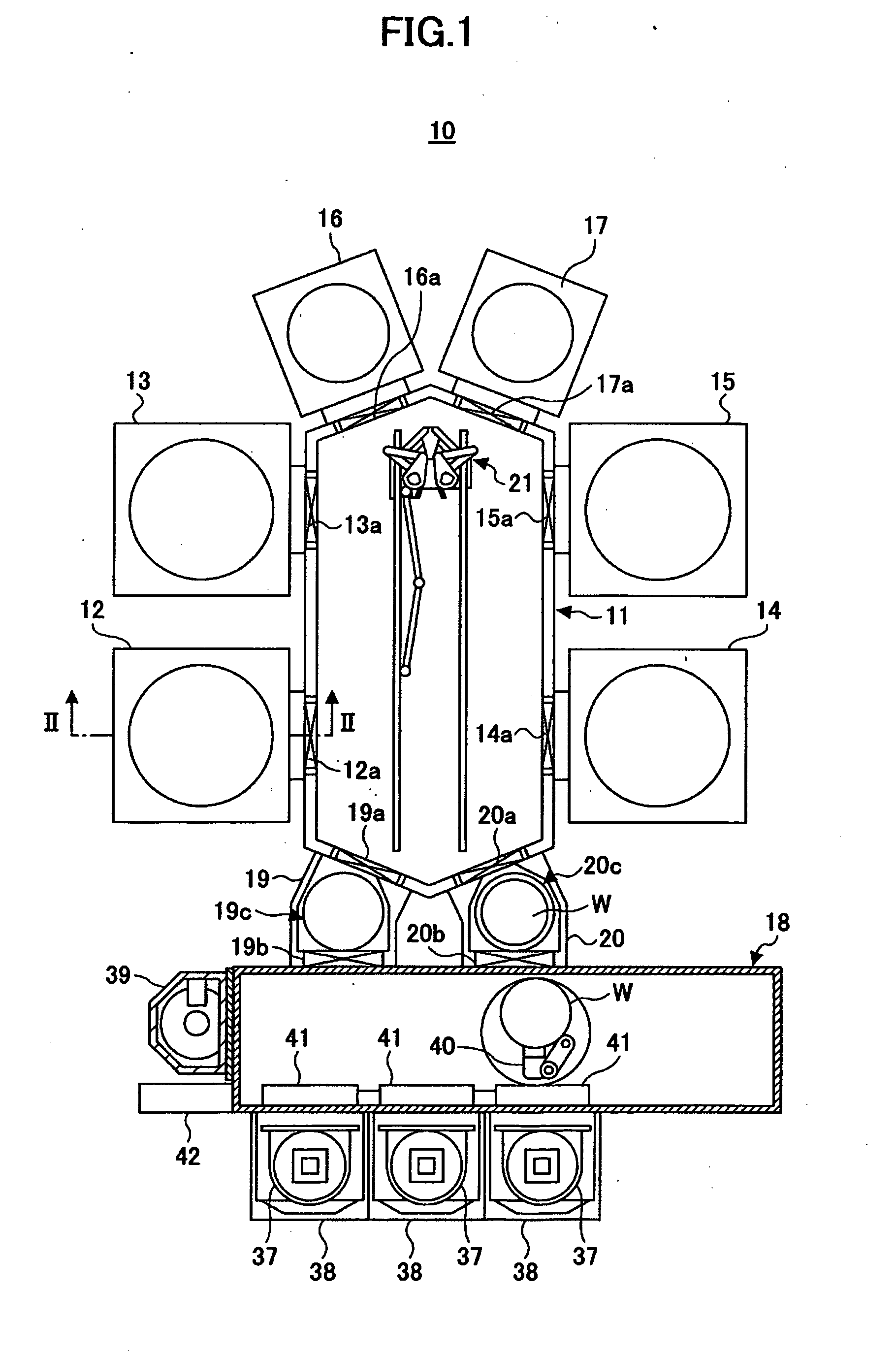
[0029]FIG. 1 is a plan view showing a schematic structure of the substrate processing system which is configured to perform the substrate processing method of this embodiment.
[0030]In FIG. 1, a substrate processing system 10 includes a transfer module 11 in a hexagon plan shape, two process modules 12 and 13 connected to one side of the transfer module 11, two process modules 14 and 15 connected to the other side of the transfer module 11 so as to oppose to the two process modules 12 and 13 respectively, a process module 16 provided adjacent to the process module 13 and connected to the transfer module 11...
second embodiment
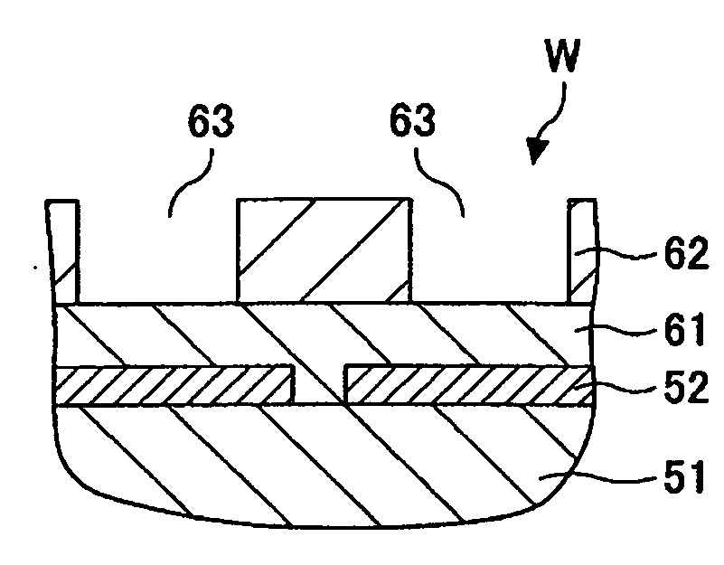
[0083]A description is made on a substrate processing method of this invention.
[0084]FIGS. 6A to 6I are process diagrams showing the substrate processing method of this embodiment. The substrate processing method of this embodiment is performed by a substrate processing system having a similar structure to the substrate processing system 10 of FIG. 1. In the substrate processing method of this embodiment, a silicon substrate 65 (process layer) such as a thermally oxidized silicon film 66 (intermediate layer) with a thickness of, for example, 100 nm, a reflection preventive film (BARC film) 67, and a photoresist film 68 (mask film) formed of KrF are stacked in this order as a wafer W. An aperture (hole or trench) with a width of about 30 nm is formed in the silicon substrate 65. In the wafer W, the photoresist film 68 is formed in a predetermined pattern, partially exposing the reflection preventive film 67. A width of the photoresist film 68 (length of horizontal direction in the dr...
third embodiment
[0095]A description is now made on a substrate processing method of this invention.
[0096]FIGS. 7A to 7F and 8A to 8F are process diagrams showing a substrate processing method of this embodiment. The substrate processing method of this embodiment is also performed by a substrate processing system having a similar structure to the substrate processing system 10 shown in FIG. 1. In the substrate processing method of this embodiment, a first polysilicon layer 72, a first TEOS film 73, a second polysilicon layer 74 (process layer), a first silicon nitride film 75 (first intermediate layer), a second TEOS film 76 (second intermediate layer), a second silicon nitride film 77 (second intermediate layer), a reflection preventive film (BARC film) 78 (third intermediate layer), and a photoresist film 79 (mask film) are stacked in this order as a wafer W. Plural apertures (holes or trenches) with a width of about 30 nm are formed in the second polysilicon layer 74 with a narrow pitch between t...
PUM
| Property | Measurement | Unit |
|---|---|---|
| Time | aaaaa | aaaaa |
| Thickness | aaaaa | aaaaa |
| Electrical conductor | aaaaa | aaaaa |
Abstract
Description
Claims
Application Information
 - R&D Engineer
- R&D Manager
- IP Professional
- Industry Leading Data Capabilities
- Powerful AI technology
- Patent DNA Extraction
Browse by: Latest US Patents, China's latest patents, Technical Efficacy Thesaurus, Application Domain, Technology Topic, Popular Technical Reports.
© 2024 PatSnap. All rights reserved.Legal|Privacy policy|Modern Slavery Act Transparency Statement|Sitemap|About US| Contact US: help@patsnap.com