
Apparatus for Charging Dry Air or Nitrogen Gas into a Container for Storing Semiconductor Wafers and an Apparatus for Thereby Removing Static Electricity from the Wafers

Inactive Publication Date: 2010-07-15
KONDO IND +1
View PDF13 Cites 25 Cited by
  • Summary
  • Abstract
  • Description
  • Claims
  • Application Information

AI Technical Summary

Benefits of technology

[0014]an apparatus for charging dry air or nitrogen gas into a container for storing semiconductor wafers without opening the lid of the container, to remove chemical gas and moisture from the container, and then to prevent the corrosion of the semiconductor wafers by preventing acid from being generated at the surfaces of the wafers, and
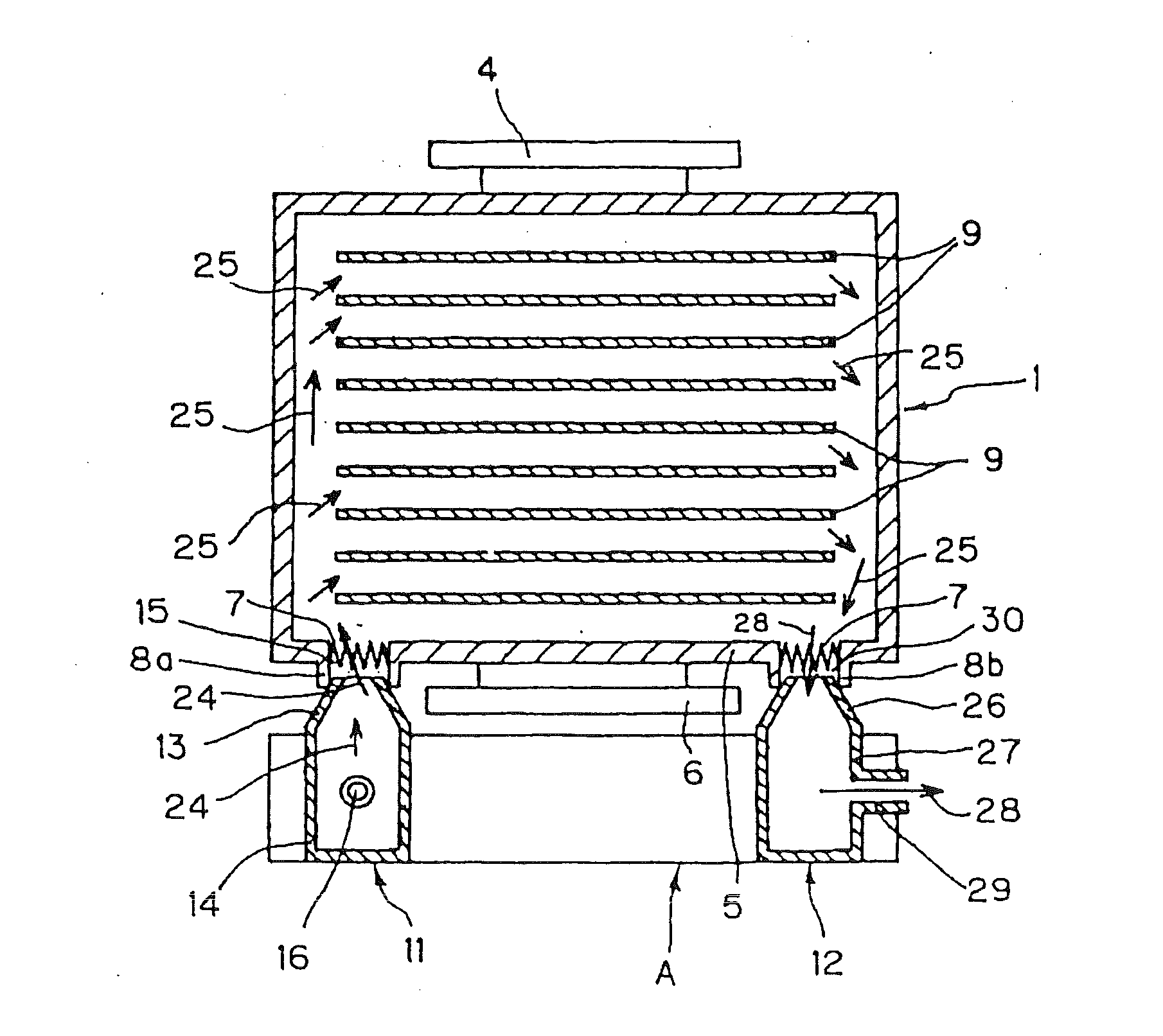
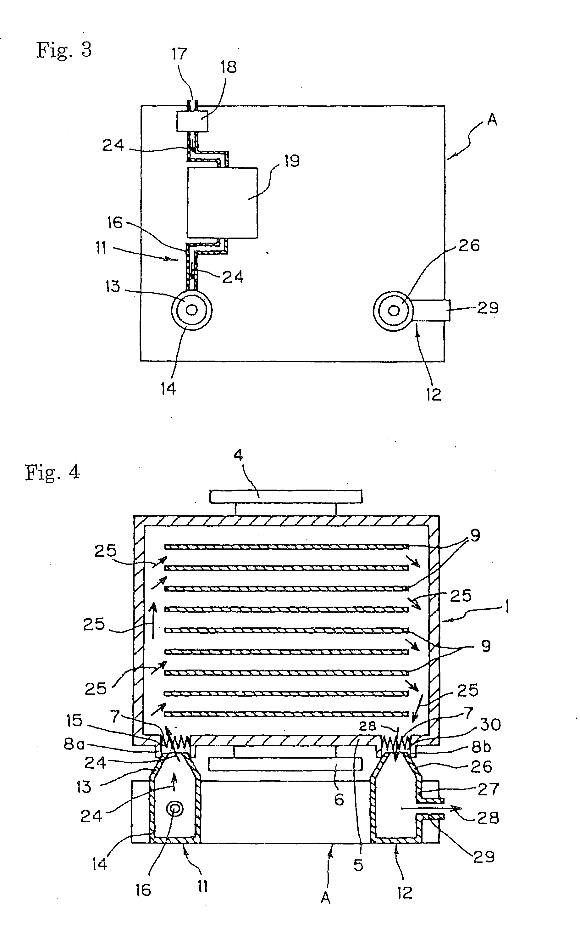
[0059]when the ionized dry air or the nitrogen gas is charged into the container for storing the semiconductor wafers from the nozzle for providing it, and until the pressure in the container increases at the initial stage, the ionized dry air or nitrogen gas is charged at a high flow rate. As the pressure in the container increases, the flow rate of the ionized dry air or nitrogen gas decreases. By installing a buffering tank on the pathway for providing the ionized dry air or nitrogen gas of the apparatus, since the flow rate of the ionized dry air or nitrogen gas that is provided to the hollow vessel disposed at the side of the intake of the container is averaged, it is possible to prevent the ionized dry air or nitrogen gas from being rapidly charged into the container. Thus, the dust that has accumulated at the bottom of the container is not stirred up.

Problems solved by technology

Further, when the semiconductor wafers are stored in the container, since the undersides of the wafers contact the surface of an arm of a robot, a small amount of dust is generated.
The dust is likely to enter the container.
Thus, there is a problem in that the dust that is caused by the above reason and by any other reason accumulates at the bottom of the container.
At the initial stage for charging dry air or nitrogen gas, there is a problem in that the dust that has accumulated at the bottom of the container or that is attached to the undersides of the wafers is stirred up, since the dry air or nitrogen gas is charged into the container at a high flow rate, and then the dust is attached to the circuits of the semiconductor at the upper surfaces of the wafers.
However, even if a mass flow meter is provided in the apparatus, the surge of the flow of the dry air or nitrogen gas cannot be avoided.
Further, since a mass flow meter is very expensive, there is a problem in that the cost of the apparatus increases.
However, the breakdown of the semiconductor circuits due to a small amount of the static electricity remaining and the attachment of the dust to the semiconductor wafers is caused.
The method for imparting electrical conductivity to the material of which the container is made by mixing a conductive material, such as a powder of carbon, with the material, cannot entirely prevent generating the static electricity toward the semiconductor wafers.
Disadvantageously, as the amount of the carbon in the material composing the container increases, the chemical gases generated from that material become a problem.
Thus, the problems of the static electricity affecting the semiconductor wafers cannot be entirely solved.

Method used


Image

  • Apparatus for Charging Dry Air or Nitrogen Gas into a Container for Storing Semiconductor Wafers and an Apparatus for Thereby Removing Static Electricity from the Wafers
  • Apparatus for Charging Dry Air or Nitrogen Gas into a Container for Storing Semiconductor Wafers and an Apparatus for Thereby Removing Static Electricity from the Wafers
  • Apparatus for Charging Dry Air or Nitrogen Gas into a Container for Storing Semiconductor Wafers and an Apparatus for Thereby Removing Static Electricity from the Wafers

Examples


embodiment 1

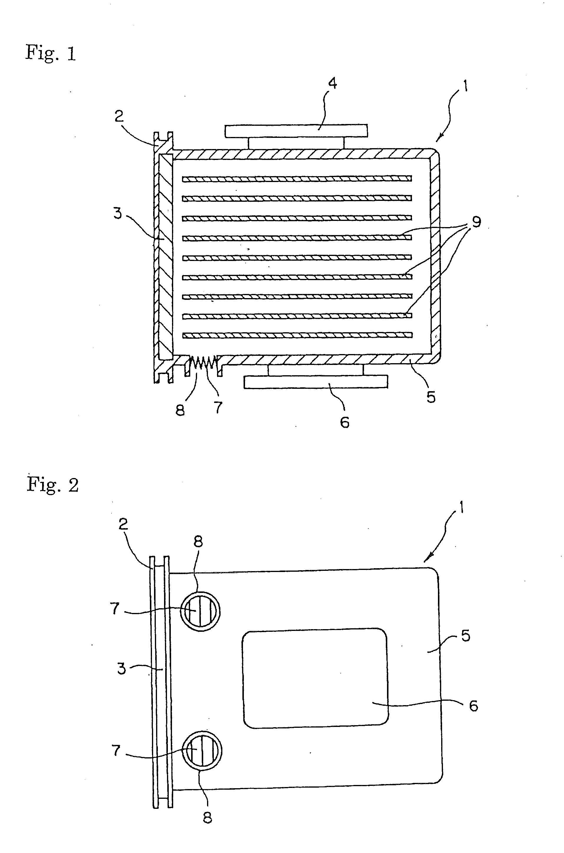
[0077]Embodiment 1 of the present inventions, the apparatus for charging dry air or nitrogen gas, is now explained in detail based on the figures. FIG. 1 shows a vertical and sectional view of the container for storing semiconductor wafers that is used for the present inventions. FIG. 2 shows a bottom plane view of the container. As shown in FIGS. 1 and 2, the container 1 for storing semiconductor wafers comprises an openable and closable lid 3 that is disposed at the front of the container. and the container 1 has a flange 2, a hook 4, for being suspended, disposed at its top plate, a leg 6 for being mounted on the table (not shown) disposed at its bottom plate 5, and a plurality of openings 8 having a PTFE filter 7.

[0078]The semiconductor wafers 9 are stored in the container 1. Except when the wafers 9 are being processed in an apparatus (not shown), since the wafers 9 are stored in the container 1, chemical gas is prevented from contacting the surfaces of the wafers 9.

[0079]FIG. ...

embodiment 2

[0094]As Embodiment 2, an apparatus for removing static electricity using the above apparatus for charging dry air or nitrogen gas, is below explained based on the figures.

[0095]FIG. 8 shows a plane view of the apparatus for removing static electricity using the apparatus for charging dry air or nitrogen gas, of this invention. FIG. 9 shows a vertical and sectional view of the apparatus for removing static electricity that is attached to the container for storing the semiconductor wafers, which is shown by FIGS. 1 and 2. As shown in FIGS. 8 and 9, the apparatus B for removing static electricity, which is used for removing the static electricity charged on the wafers 9 in the container 1, comprises:

[0096]a portion 11a for providing ionized dry air or nitrogen gas to charge the ionized dry air or nitrogen gas into the container 1, which portion 11a uses a portion 11 for providing the dry air or nitrogen gas of the apparatus A,

[0097]a portion 12a for exhausting the used ionized dry air...


PUM


Abstract

An apparatus for charging dry air or nitrogen gas into a container for storing semiconductor wafers can remove chemical gas and moisture from the container, and then prevent acid from being generated at the surfaces of the wafers.The apparatus A for charging dry air or nitrogen gas into a container 1 for storing semiconductor wafers 9 is connected to an opening 8a, acting as an intake, and to an opening 8b, acting as an exhaust, wherein the container 1 comprises a plurality of openings 8 disposed at the bottom plate of the container 1, the apparatus comprising:PTFE filters 7 disposed at the plurality of openings 8a, 8b, a portion 11 for providing the dry air or nitrogen gas to the container 1, anda portion 12 for exhausting the used dry air or nitrogen gas from the container 1 after removing chemical gas and moisture from the container, and then preventing acid from being generated at the surfaces of the wafers 9.

Description

TECHNICAL FIELD[0001]This invention relates to an apparatus for charging dry air or nitrogen gas into a container for storing semiconductor wafers and an apparatus for removing static electricity from the surfaces of the wafers by using the apparatus for charging dry air or nitrogen gas. The container is used for storing semiconductor wafers that are used for producing semiconductor chips. Since any chemical gas or moisture present in the container can be removed by charging dry air or nitrogen gas into the container, it is possible to prevent an acid from being generated at the surfaces of the wafers.BACKGROUND OF THE INVENTION[0002]Conventionally, for processes for producing semiconductor chips in a clean room using a minienvironment system, since miniaturization of the circuits of the semiconductor chips had been developed, the processes have become complicated. Particularly, for a process for etching semiconductor wafers by using halogen gases, since an acid is generated by a ch...

Claims


Application Information

Patent Timeline
IPC IPC(8): B65B31/04
CPCH01L21/67017H01L21/68H01L21/67396H01L21/67393
Inventor KISAKIBARU, TOSHIROUOKADA, MAKOTOIIDA, NAOJIHONDA, YASUSHI
Owner KONDO IND
Learn More