

Method for reducing tip-to-tip spacing between lines
a technology of lithography and line spacing, which is applied in the direction of photosensitive material processing, photomechanical equipment, instruments, etc., can solve the problems of increasing unit cell density, shrinking device dimensions, and currently available lithographic techniques that cannot achieve a tip-to-tip distance of not less than 100 nm, and achieve the effect of reducing tip-to-tip spacing
- Summary
- Abstract
- Description
- Claims
- Application Information
AI Technical Summary
Benefits of technology
Problems solved by technology
Method used
Image

Examples
Embodiment Construction
[0025]In describing the preferred embodiments of the present invention, reference will be made herein to FIGS. 1A-23B of the drawings in which like numerals refer to like features of the invention. Features of the invention are not necessarily shown to scale in the drawings.
[0026]It is understood that when an element, such as a layer, region or substrate, is referred to as being “on” or “over” another element, it can be directly on the other element or intervening elements may also be present.
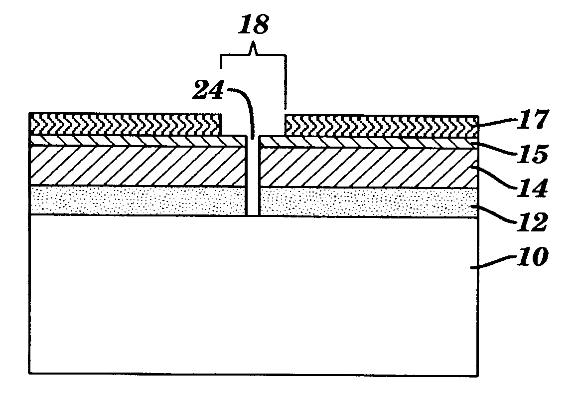
[0027]The present invention combines the conventional photolithography technology with the copolymer self-assembling lithographic techniques to reduce tip-to-tip spacing between lines.
[0028]Specifically, a mask layer is first formed over the substrate containing a line structure. A trench opening is then created in the mask layer by conventional lithography and etch techniques. Such a trench opening has a relatively large width d which is consistent with the resolutions of the conventional lith...
PUM
 Abstract
Description
Claims
Application Information