High Margin Multilevel Phase-Change Memory via Pulse Width Programming

a phase-change memory and pulse width technology, applied in the field of phase-change memory material programming, can solve the problems of limited progress toward achieving a practical multi-level phase-change memory, reproducibility is particularly difficult, and the resistance of the programmed state is becoming increasingly difficult to employ, so as to achieve fine control of the crystalline-amorphous structural transformation, increase the number of practical programming states, and control the resistivity of the programmed state.

Inactive Publication Date: 2010-07-22
OVONYX
View PDF5 Cites 31 Cited by
  • Summary
  • Abstract
  • Description
  • Claims
  • Application Information

AI Technical Summary

Benefits of technology

[0015]The invention further includes a method of programming a phase-change device to control the sensitivity of programmed resistance to programming conditions. The method includes controlling the resistivity of the programmed state by varying the duration of the electrical pulses used to program the device. In one embodiment, programming to different resistance states occurs by fixing the amplitude of the programming pulse

Problems solved by technology

Miniaturization has been a successful strategy for increasing storage density over the past few decades, but is becoming increasingly more difficult to employ as fundamental size limits of manufacturability are reached.
Although phase-change memory offers the potential for multiple bit operation, progress toward achieving a practical multilevel phase-change memory has been limited.
One of the practical complications associated with multilevel phase-change operation is achieving adequate resolution of the different memory states with respect to a programming variable.
Another practical complication is a need to achieve reproducible programming to targeted memory states.
Reproducibility poses a particular challenge in the face of the normal variations in the programming conditions that accompany memory ope

Method used


Image

  • High Margin Multilevel Phase-Change Memory via Pulse Width Programming
  • High Margin Multilevel Phase-Change Memory via Pulse Width Programming
  • High Margin Multilevel Phase-Change Memory via Pulse Width Programming

Examples


example i

[0062]In this example, the effect of pulse width on the programmed resistance of a phase-change device having a lower electrode with low resistivity is described.

[0063]FIG. 5 depicts a typical phase-change memory device 100 that includes base wafer 110, dielectric buffer 120, lower electrode 130, conductive line 140, dielectric 150, phase-change material 160, dielectric 170, upper electrode 180, and conductive line 190. Conductive lines 140 and 190 receive and deliver electrical signals to surrounding circuitry and may, for example, be a word line and a bit line of a memory device in an array. In device 100, current is delivered from an external device through conductive line 140 and lower electrode 130 to phase-change material 160 and upper electrode 180 and conductive line 190. Phase-change material 160 has the composition Ge2Sb2Te5. The direction of current flow in device 100 is generally vertical between the portion of lower electrode 130 in contact with phase-change material 16...

example ii

[0069]In this example, the effect of pulse width on the programmed resistance of a phase-change device having a lower electrode with high lateral resistivity is described.

[0070]FIG. 7 shows a device structure 200 utilizing a lower electrode having a high resistance to lateral flow of electrical or thermal energy. Device 200 includes base wafer 205, conductive line 210, lower electrode 215, and dielectric 220 having an opening formed therein. Breakdown layer 225 and phase-change material 230 are formed within the opening. Phase-change material 230 is also formed over the opening and on dielectric 220. Device 200 further includes upper electrode 235, metal layers 240 and 250, surrounding dielectric 245, and conductive line 255. Phase-change material 230 has the composition Ge2Sb2Te5 and breakdown layer 225 is a thin insulating layer (having a thickness of ˜10-30 Å).

[0071]In device 200, current is delivered from an external device through conductive line 210 to lower electrode 215 and ...

example iii

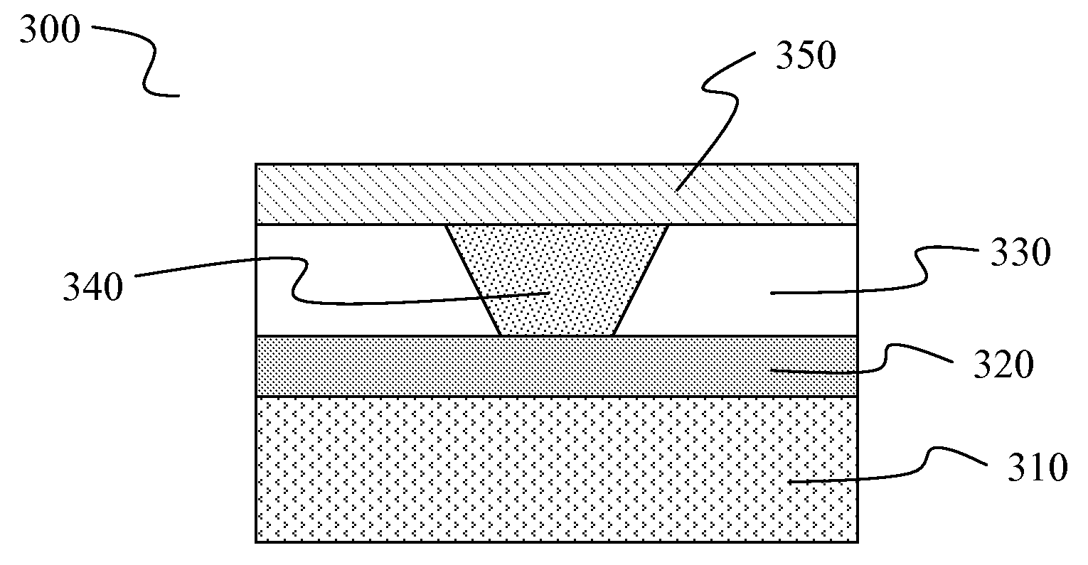
[0078]In this example, the effect of programming pulse width on the resistance of a device in accordance with the instant invention is described. The device is shown as device 300 in FIG. 9. Device 300 includes base wafer 310, lower electrode 320, phase-change material 340 positioned within an opening of surrounding dielectric 330, and upper electrode 350. Phase-change material 340 is Ge2Sb2Te5. In device 300, current is delivered from an external device through a conductive line connected to lower electrode 320 and continues through phase-change material 340 to upper electrode 350.

[0079]Lower electrode 320 is an intermediate resistivity form of TiAlN obtained by annealing TiAlN at 400° C. The resistivity of the annealed electrode material is ˜3-6 mΩ-cm. Other electrode materials (e.g. TiSiN, TiW, TiN, MoN, nitrogenated carbon) provide a resistivity in a range providing the benefits of the instant invention if annealed to a temperature appropriate for the material. The resistivity o...


PUM


Abstract

An electronic device and method of programming for binary and multilevel memory operation. The active material of the device is a phase-change material. The method includes utilization of the pulse duration of electrical pulses as a programming variable to program a phase-change device to two or more memory states that differ in the relative proportion and/or spatial arrangement of crystalline and amorphous phase regions. Pulse width programming, in conjunction with a device electrical contact having a resistivity within a particular range, enables fine control over the crystalline-amorphous phase-change process by facilitating control over the spatial distribution of thermal energy produced by Joule heating. The degree of control over the phase-change process enables reliable multilevel memory operation by providing for reproducible programming of memory states that are well-resolved in both resistance and programming variable.

Description

FIELD OF INVENTION[0001]This invention relates to the programming of variable resistance memory materials. More particularly, this invention relates to the programming of phase-change memory materials for multilevel operation. Most particularly, this invention relates to programming reliability of multilevel phase-change memory devices and the use of programming pulse width at particular currents to provide greater margin in the programming current required to achieve the individual states in a multilevel memory device.BACKGROUND OF THE INVENTION[0002]Variable resistance materials are promising active materials for next-generation electronic storage and computing devices. The central feature of a variable resistance material is its ability to adopt two or more distinguishable states that differ in electrical resistance. A variable resistance material can be programmed back and forth between the distinguishable states by providing energy or power. The applied energy or power induces ...

Claims


Application Information

Patent Timeline
IPC IPC(8): G11C11/00
CPCG11C11/5678G11C13/0004G11C13/0069G11C2013/0083G11C2013/0092
Inventor KOSTYLEV, SERGEYLOWREY, TYLER
Owner OVONYX
Why Eureka
Try Eureka