Method of Forming Conformal Dielectric Film Having Si-N Bonds by PECVD

a dielectric film and conformal technology, applied in the direction of semiconductor/solid-state device details, coatings, chemical vapor deposition coatings, etc., can solve the problems of poor conformality or poor step coverage on a substrate containing small and/or high aspect ratio features, and poor conformal coverage can hamper the development of higher density circuit devices and elements

Active Publication Date: 2010-07-22
ASM JAPAN
View PDF13 Cites 398 Cited by
  • Summary
  • Abstract
  • Description
  • Claims
  • Application Information

AI Technical Summary

Benefits of technology

[0008]An object of at least one embodiment of the present invention is to provide a method of forming a hydrogen-containing conformal layer having Si—

Problems solved by technology

However, the PECVD method for forming silicon nitride leads to poor conformality or poor step coverage on a substrate containing small and/or high aspect ratio features.
In smal

Method used


Image

  • Method of Forming Conformal Dielectric Film Having Si-N Bonds by PECVD
  • Method of Forming Conformal Dielectric Film Having Si-N Bonds by PECVD
  • Method of Forming Conformal Dielectric Film Having Si-N Bonds by PECVD

Examples


example 1

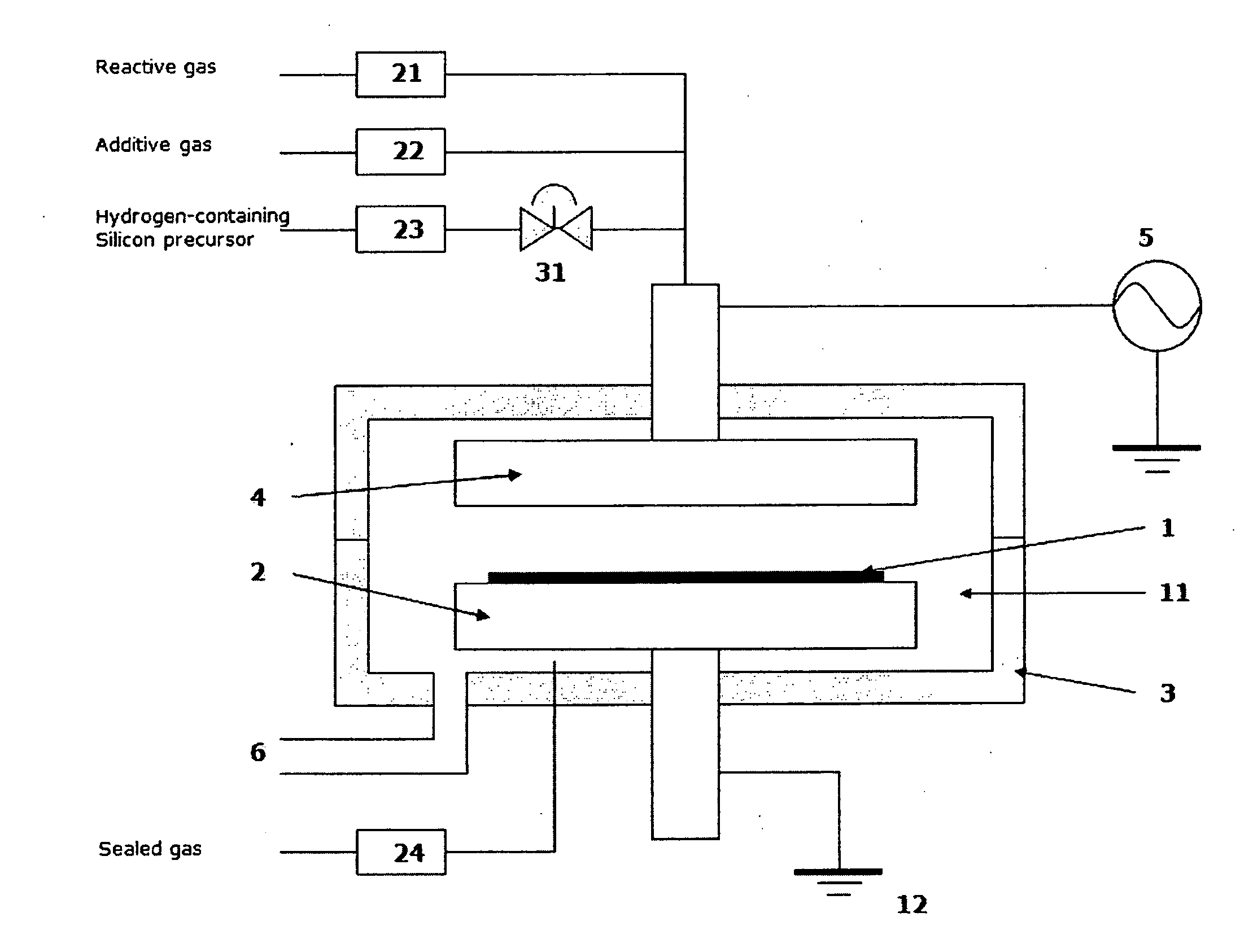
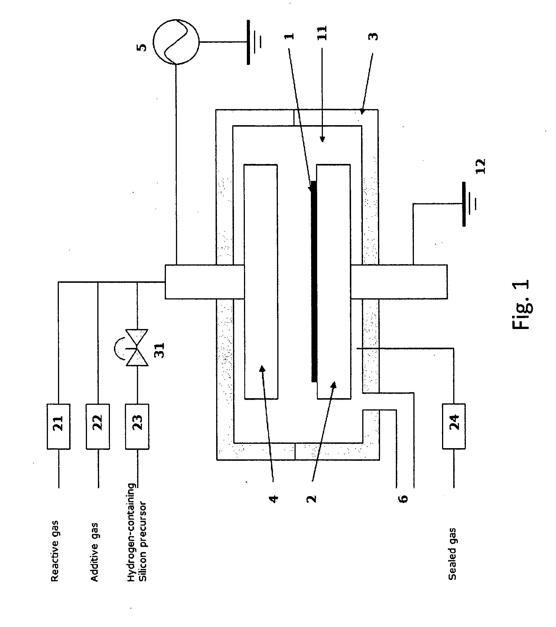
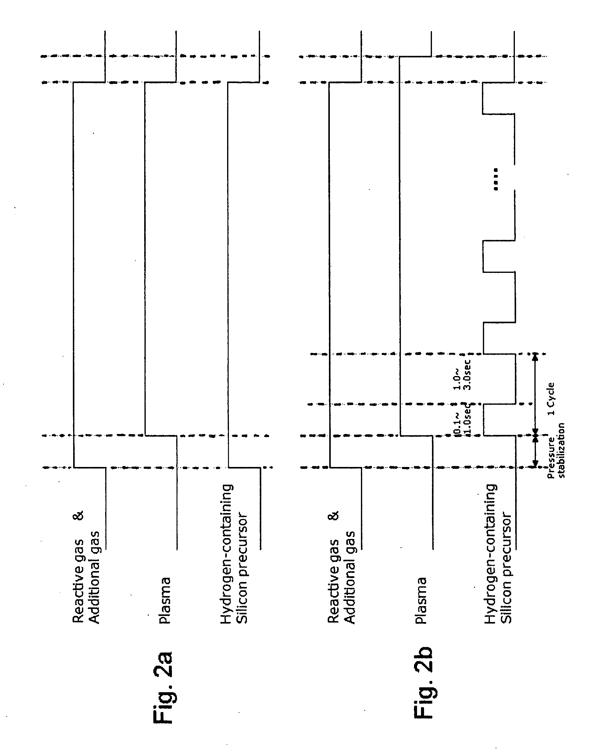
[0070]An insulative silicon nitride layer was formed on a substrate having trenches under the conditions shown below using the sequence illustrated in FIG. 2b and the PECVD apparatus illustrated in FIG. 1. The trenches included relatively wide trenches (a width of 500 nm and a depth of 350 nm) and relatively narrow trenches (a width of 50 nm and a depth of 350 nm). Thus trenches of different aspect ratio were coated.

[0071]Silane: 50 sccm

[0072]Hydrogen: 1000 sccm

[0073]Nitrogen: 2000 sccm

[0074]Process helium: 2000 sccm

[0075]Sealed helium: 500 sccm

[0076]Argon: 100 sccm

[0077]Substrate Temp.: 300° C.

[0078]RF power (a frequency of 13.56 MHz): 0.12 W / cm2

[0079]Pressure: 6 Torr

[0080]Silane supply time: 1 sec supply, 3 sec supply stop

[0081]After completion of the deposition, the trenches were observed with a scanning electron microscope.

[0082]It was confirmed that the step coverage (conformality) was more than 80% (80%-87%), defined as the ratio between the thickness of the sidewall to the t...

example 2

[0083]An insulative silicon nitride layer was formed on a substrate having trenches under the conditions shown below using the sequence illustrated in FIG. 2b and the PECVD apparatus illustrated in FIG. 1. The trenches included relatively wide trenches (a width of 500 nm and a depth of 350 nm) and relatively narrow trenches (a width of 50 nm and a depth of 350 nm).

[0084]Trisilylamine: 300 sccm

[0085]Hydrogen: 500 sccm

[0086]Nitrogen: 1000 sccm

[0087]Process helium: 1400 sccm

[0088]Sealed helium: 500 sccm

[0089]Argon: 500 sccm

[0090]Substrate temp.: 300° C.

[0091]RF power (a frequency of 13.56 MHz): 0.12 W / cm2

[0092]Pressure: 6 Torr

[0093]Trisilylamine supply time: 0.2 sec supply, 2 sec supply stop

[0094]After completion of the deposition, the trenches were observed with a scanning electron microscope (SEM).

[0095]FIGS. 3a and 3b show the scanning electron microscope cross-sectional view of the substrate with the conformal silicon nitride layer formed. Qualitatively, the silicon nitride layer ...


PUM

PropertyMeasurementUnit
Temperatureaaaaaaaaaa
Fractionaaaaaaaaaa

Abstract

A method of forming a conformal dielectric film having Si—N bonds on a semiconductor substrate by plasma enhanced chemical vapor deposition (PECVD) includes: introducing a nitrogen- and hydrogen-containing reactive gas and an additive gas into a reaction space inside which a semiconductor substrate is placed; applying RF power to the reaction space; and introducing a hydrogen-containing silicon precursor in pulses into the reaction space wherein a plasma is excited, thereby forming a conformal dielectric film having Si—N bonds on the substrate.

Description

BACKGROUND [0001]1. Field of the Invention[0002]The present invention relates to semiconductor integrated circuit manufacturing and, more particularly to a method of forming a conformal dielectric film such as a silicon nitride film.[0003]2. Description of the Related Art[0004]In integrated circuits fabricated on semiconductor substrates for large scale integration require multiple levels of metal interconnections to electrically interconnect discrete layers of semiconductor devices formed on semiconductor chips. The different levels of interconnections are separated by various insulating or dielectric layers, which are etched to form via holes so as to connect one level of metal to another.[0005]The evolution of chip design continually requires faster circuitry and greater circuit density than before. For faster circuits with greater circuit densities, certain properties are required of materials used to fabricate such integrated circuits, particularly as the dimensions of integrat...

Claims


Application Information

Patent Timeline
IPC IPC(8): H01L21/469
CPCC23C16/045C23C16/345C23C16/45523H01L21/0217H01L21/02211H01L21/02219H01L21/02274H01L21/0228H01L21/3185
Inventor LEE, WOO JINSHIMIZU, AKIRAFUKAZAWA, ATSUKI
Owner ASM JAPAN
Why Eureka
Try Eureka