Compound semiconductor epitaxial wafer and fabrication method thereof

Inactive Publication Date: 2010-07-29
PACIFIC SPEED
View PDF2 Cites 4 Cited by
  • Summary
  • Abstract
  • Description
  • Claims
  • Application Information

AI Technical Summary

Benefits of technology

[0006]Therefore, it is a primary objective of the present invention to provide a high-quality compound semiconductor epitaxial wafer and a fabrication method thereof, wherein an improved metal substrate is used, and an improved processes for the epitaxial wafer structure and the thermal cycle of annealing heat treatment process are adopted to achieve the effects of improving the quality of crystals, simplifying the process, and lowering the cost.
[0012]In the present invention, a metal substrate of the Group III˜V compound semiconductor is used to provide the advantages of a flexible size of the substrate, a low cost, a high heat dissipating, a highly bendable feature and a high carrier mobility, and thus the invention can be applied extensively in the areas of large building curtains, electric cars and 3C products, and comes with a cost much lower than the Group III˜V compound semiconductor substrate using a silicon substrate, so as to achieve a high heat dissipation and a low manufacturing cost for components such as light emitting diodes, photodiodes, solar cells, laser diodes or high power transistors, etc.
[0013]In the heat treatment process of the invention, the first silicon buffer layer, the second compound semiconductor buffer layer and the third compound semiconductor buffer layer are working together to reduce the probability of the occurrence of threading dislocations, so as to obtain a better-quality compound semiconductor epitaxial wafer.

Problems solved by technology

Therefore, the Group III˜V compound semiconductor epitaxial wafer on the buffer layer usually forms a threading dislocation in the compound semiconductor epitaxial layer due to the unmatched lattices and the different thermal expansion coefficients, and gives rise to a poor quality of crystals.

Method used


Image

  • Compound semiconductor epitaxial wafer and fabrication method thereof
  • Compound semiconductor epitaxial wafer and fabrication method thereof
  • Compound semiconductor epitaxial wafer and fabrication method thereof

Examples


Embodiment Construction

[0018]Other features and advantages of the present invention will become apparent in the following detailed description of the preferred embodiments with reference to the accompanying drawings.

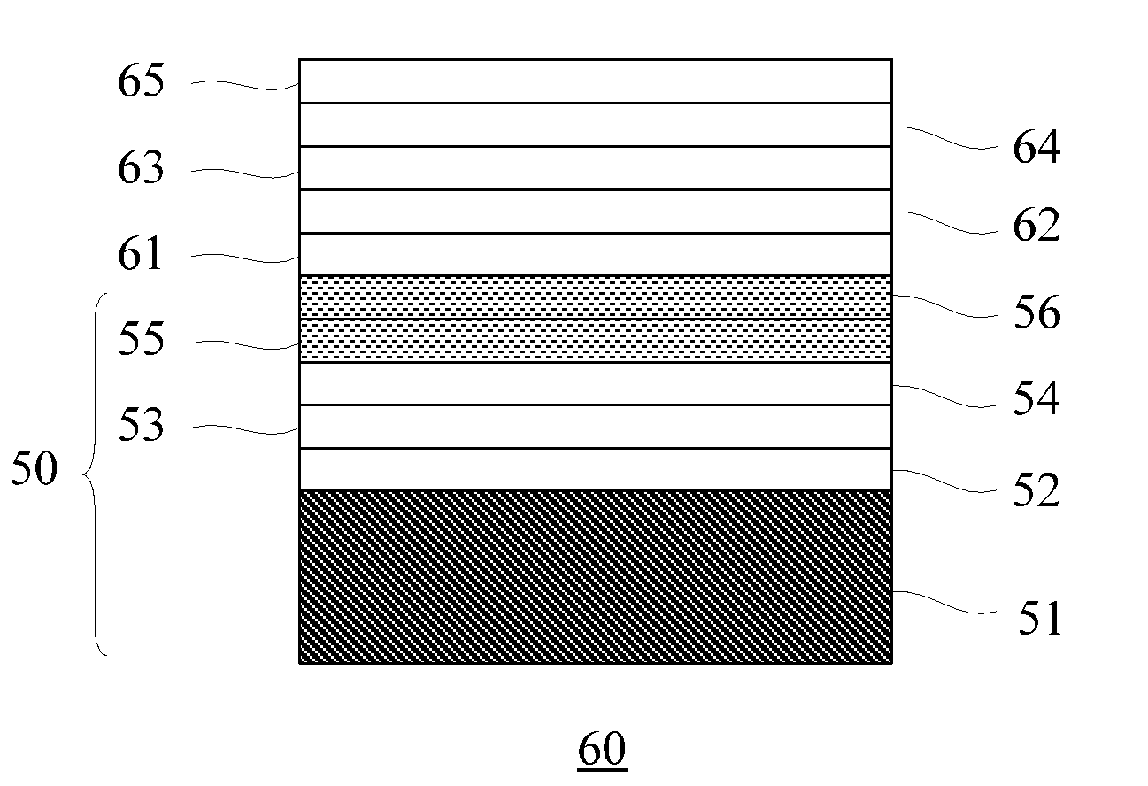
[0019]With reference to FIG. 1 for a cross-sectional view of a compound semiconductor epitaxial wafer 50 in accordance with a preferred embodiment of the present invention, a metal-organic chemical vapor deposition process is adopted as the deposition process, and a molecular beam epitaxial process is adopted as an epitaxial process during the crystal growth process, and the compound semiconductor thin film layer is made of gallium arsenide (GaAs). Firstly, a deposition process is conducted on a metal substrate 51 in a crystal growth system, and silane (SiH4) is used as a reacting gas, and the deposition temperature is approximately equal to 580° C.˜600° C., and a silicon thin film with a thickness approximately equal to 15 Ř25 Å is deposited on the metal substrate 51, and the silicon thin fi...


PUM


Abstract

The present invention provides a compound semiconductor epitaxial wafer and a fabrication method thereof, a first silicon buffer layer is deposited on a metal substrate, and then a second compound semiconductor buffer layer is deposited on the first silicon buffer layer, and a third compound semiconductor buffer layer is deposited on the second compound semiconductor buffer layer, and a first compound semiconductor epitaxial layer is crystallized on the third compound semiconductor buffer layer, and a first thermal treatment process is applied, and a second compound semiconductor epitaxial layer is crystallized on the first compound semiconductor epitaxial layer, and a second thermal treatment process is applied to obtain a good-quality compound semiconductor epitaxial wafer.

Description

FIELD OF THE INVENTION[0001]The present invention relates to a compound semiconductor and a fabrication method thereof, and more particularly to a compound semiconductor epitaxial wafer grown on a metal substrate and a fabrication method thereof.BACKGROUND OF THE INVENTION[0002]As optoelectronic and communication industries advance rapidly, compound semiconductors of Groups III˜V compounds such as, GaAs become a major substrate for manufacturing optoelectronic and communication components due to its advantages of having a direct band-gap and a high carrier mobility and providing a material with different band-gaps obtained by a chemical reaction of different Group III˜V compounds.[0003]The optoelectronic and communication components made of the Group III˜V compound semiconductors mainly use Group III˜V compounds such as, gallium arsenide (GaAs), gallium phosphide (GaP) and indium phosphide (InP) as a substrate for an epitaxial growth under the matched lattice condition. At present, ...

Claims


Application Information

Patent Timeline
IPC IPC(8): H01L29/12H01L21/20
CPCH01L21/02425H01L21/02461H01L21/02463H01L31/101H01L21/02543H01L21/02546H01L21/0262H01L21/02505
Inventor LIN, CHIEN-FENG
Owner PACIFIC SPEED
Why Eureka
Try Eureka