

Semiconductor device having electro-static discharge protection element
- Summary
- Abstract
- Description
- Claims
- Application Information
AI Technical Summary
Benefits of technology
Problems solved by technology
Method used
Image

Examples
exemplary embodiment 1
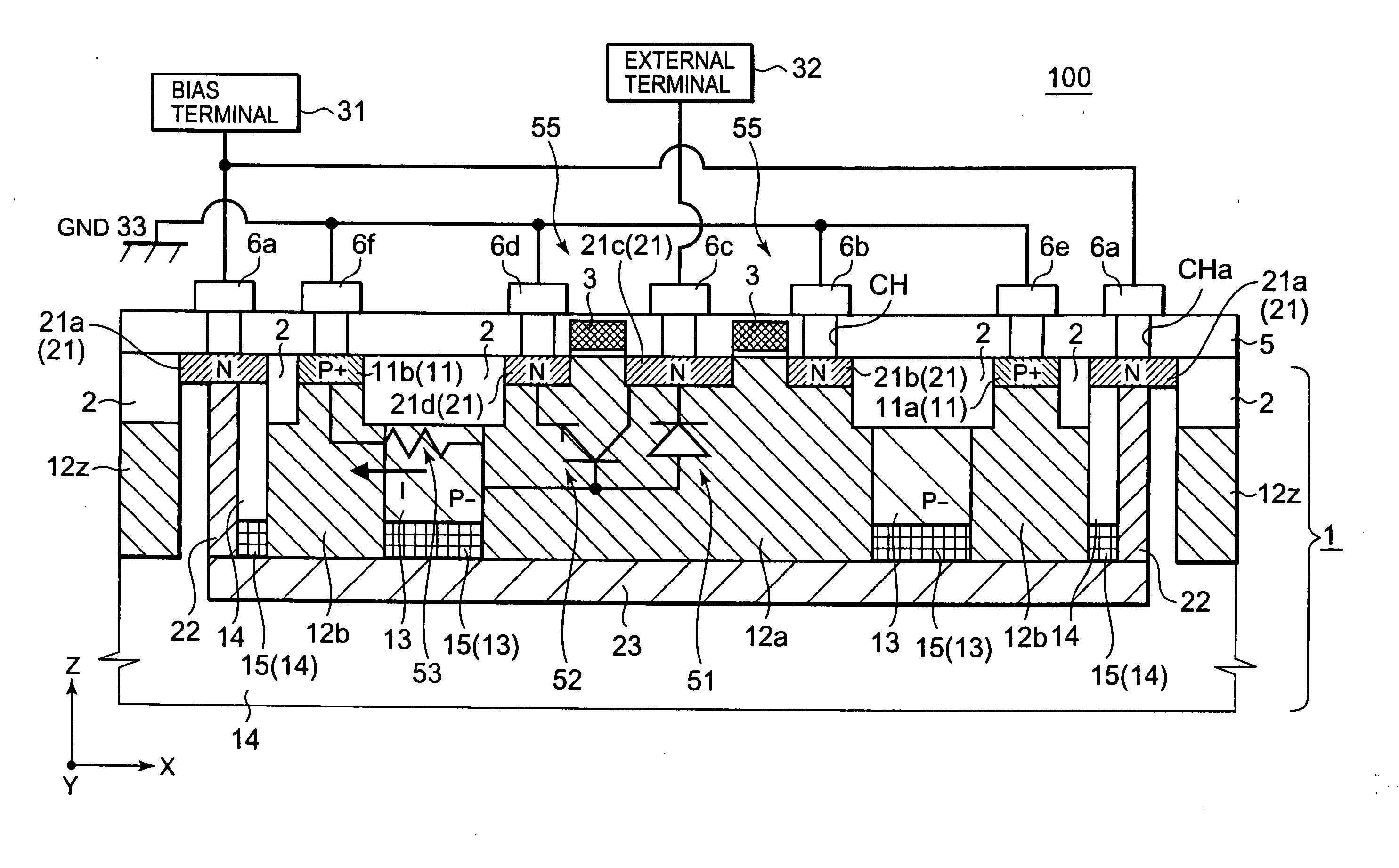
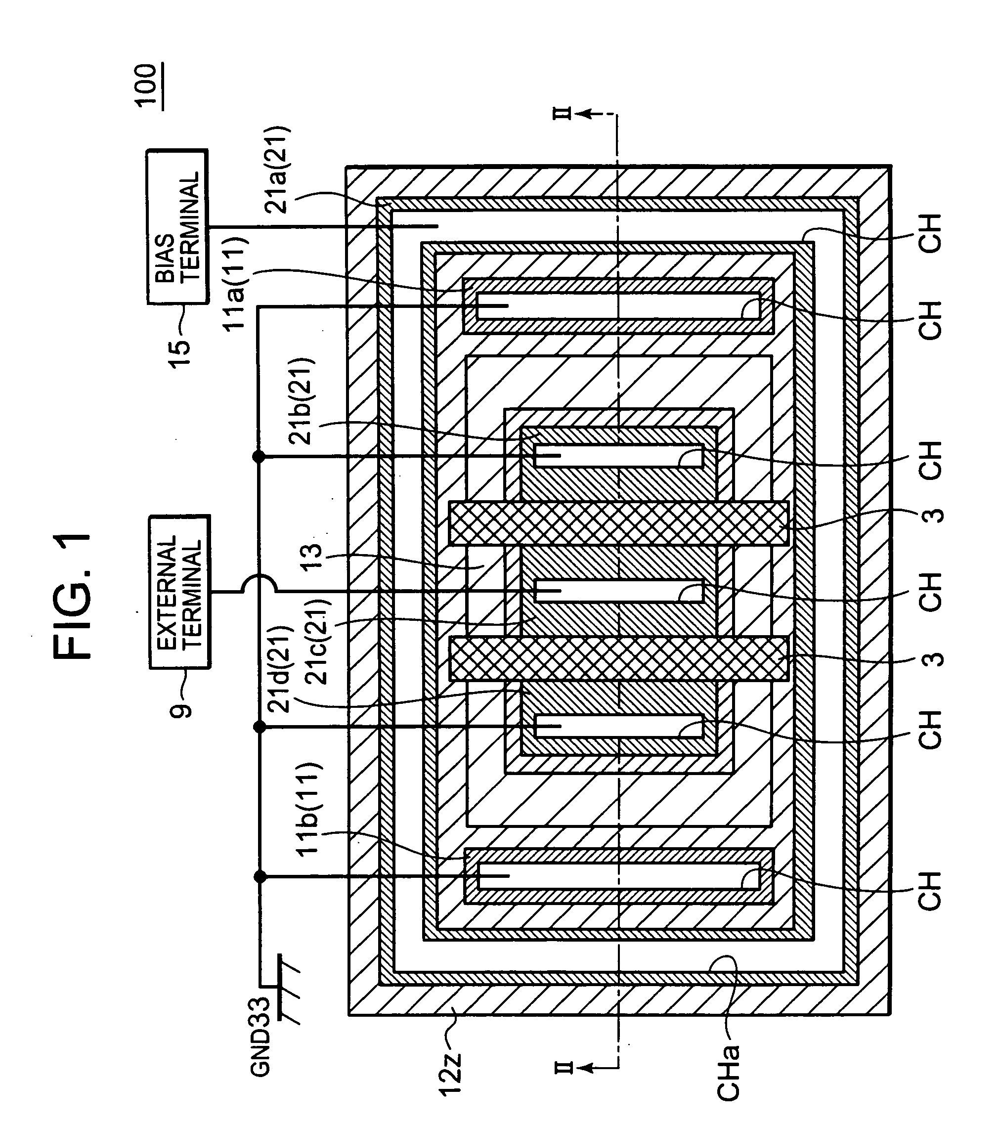
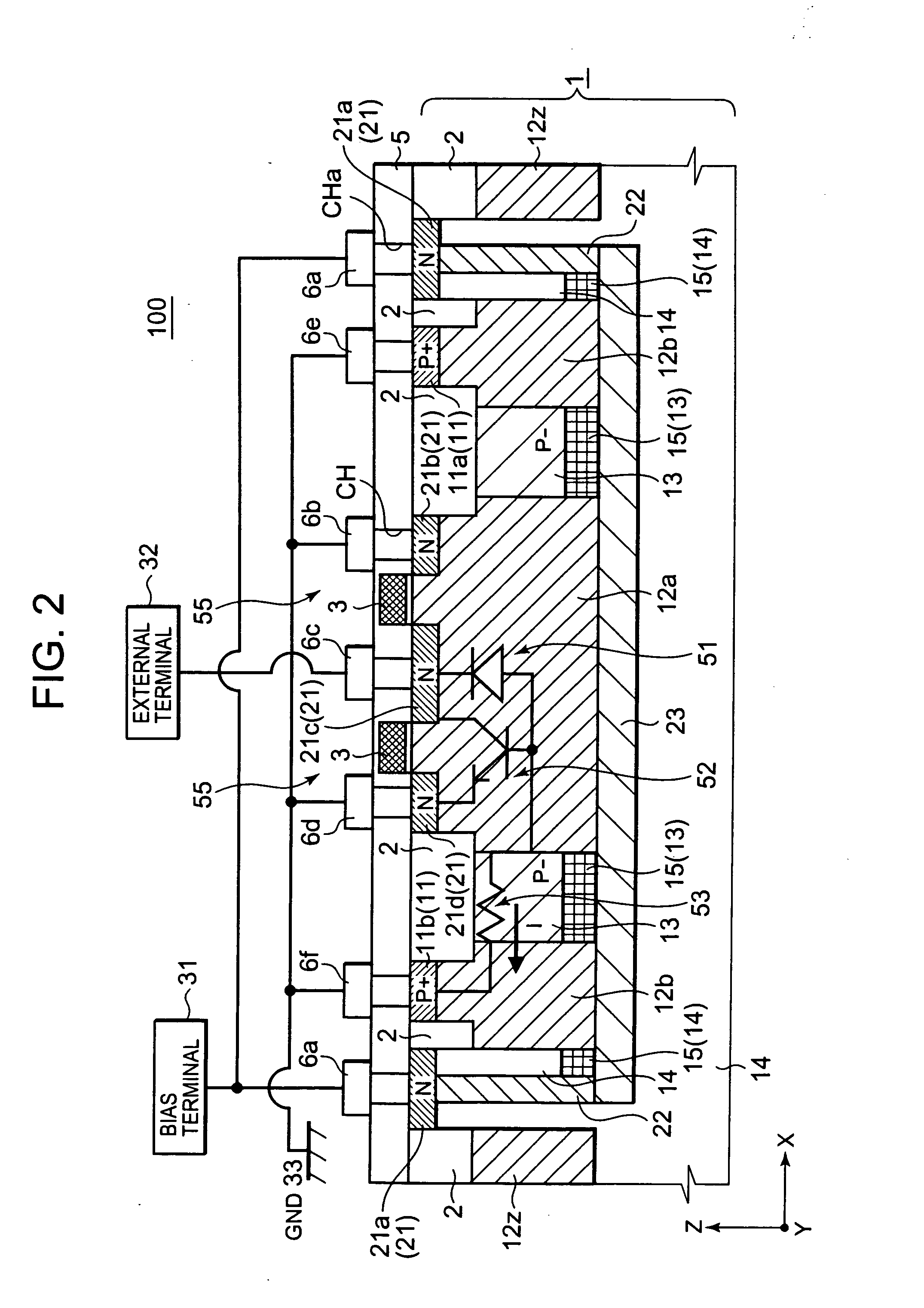
[0034]FIG. 1 shows a schematic plan view of a semiconductor device 100 which includes an ESD protection element according to exemplary embodiment 1. FIG. 2 shows a cross-sectional view of the semiconductor device 100 taken along the II-II line of FIG. 1. Note that illustrations of a field oxide film 2, an interlayer dielectric 5 and the like are omitted from FIG. 1 for the sake of explanatory convenience whereas positions of contact holes are illustrated in FIG. 1. The same is the case with the plan views coming after FIG. 1.
[0035]As shown in FIG. 2, the semiconductor device 100 includes a P type semiconductor substrate 1 (hereinafter referred to as a “substrate 1” as well) configured to function as a first conductivity-type semiconductor substrate. As shown in FIGS. 1 and 2, formed in the substrate 1 are: P+ type semiconductor diffusion regions (hereinafter referred to as “P+ type diffusion regions”) 11 (11a, 11b) as P type regions; P+ type wells 12 (12a, 12b, 12z) configured to fu...
exemplary embodiment 2
[0062]Next, descriptions will be provided for an example of a semiconductor device including an ESD protection element which is different from the ESD protection element according to the exemplary embodiment 1. The semiconductor device according to an exemplary embodiment 2 is the same as the semiconductor device according to the exemplary embodiment 1 in terms of the basic configuration and the manufacturing method, except for the following point. Specifically, what is different is that, the first P type well and the second P type well are connected together by connectors (other P type wells) in a case of the P type wells according to the exemplary embodiment 2 whereas the first P type well 12a and the second P type well 12b constituting the P type wells 12 according to the exemplary embodiment 1 are completely separated from each other with the P− type diffusion region 13 interposed in between. In other words, the P− type diffusion region 13 according to the exemplary embodiment 2...
exemplary embodiment 3
[0069]A semiconductor device according to an exemplary embodiment 3 is the same as the semiconductor device according to the exemplary embodiment 2 in terms of the basic configuration and the manufacturing method, except for the following point. Specifically, what is different is that the N type diffusion region 21a according to the exemplary embodiment 3 is connected to an external terminal 32(3) through the upper layer interconnection 6a connected to a diode, which is further connected to the external terminal 32(3), whereas the N type diffusion region 21a according to the exemplary embodiment 2 is connected to the bias terminal 15 through the upper layer interconnection 6a.
[0070]FIG. 7 shows a schematic plan view of the semiconductor device 100(3) which includes an ESD protection element according to the exemplary embodiment 3. FIG. 8 shows a cross-sectional view taken along the VIII-VIII line of FIG. 7.
[0071]The N type diffusion region 21a shaped like the frame body is electric...
PUM
 Abstract
Description
Claims
Application Information