Semiconductor Flip-Chip System Having Oblong Connectors and Reduced Trace Pitches

a technology of oblong connectors and flip-chips, which is applied in the direction of semiconductor devices, semiconductor/solid-state device details, electrical equipment, etc., can solve the problem of shortening the fine-pitch adjacent trace, and achieve the effect of enhancing the robustness of the solder joint, minimizing the risk of shortening the adjacent trace, and reducing the pitch of the connector

Active Publication Date: 2010-08-05
TEXAS INSTR INC
View PDF8 Cites 74 Cited by
  • Summary
  • Abstract
  • Description
  • Claims
  • Application Information

AI Technical Summary

Benefits of technology

[0005]The ongoing market trend of semiconductor products for higher numbers of input / output terminals at reduced product sizes demands substrate trace pitches centerline-to-centerline considerably smaller than the presently achievable 40 μm, and further reliable flip-chip contacts to these fine-pitch traces. Applicants realized that for the bumps with circular cross sections, as presently employed for flip-chip assembly, only a segment of the circular cross section is utilized for actual contact to the trace, while the rest is overhang over the trace outline. Applicants discovered that by capillary action, this overhang may pull in so much liquid solder that the solder may protrude from the overhang and thus cause a short to the fine-pitch adjacent trace.
[0006]Applicants solved the problem of risking shorts between fine-pitch adjacent substrate traces during the solder reflow phase in the bump attachment process by selecting an oblong cross section for the bumps, with the long axis (for instance, 40 to 50 μm) in line with the trace and the short axis (for instance, 20 to 25 μm) about equal to the trace width. In this solution, the actual contact between bump and trace is about equal to the bump cross section, with only negligible overhang. The lack of overhang means an absence of capillary action for the liquid solder and thus a lack of solder spilling; the risk of a short to the adjacent trace is minimized. This, in turn, means that the pitch between traces can safely shrink, for instance, to 30 μm. Furthermore, since the oblong bump cross section makes the circular cross section obsolete, the traces may feature straight outlines and avoid the present castellated (neckdown) contours. The positioning of the pillars may remain staggered, but the pitch can also shrink (for instance, to 60 μm).
[0007]Applicant further discovered that oblong bump cross sections allow the enlargement of the actual flip-chip capture areas; enlarged solder joints, in turn, enhance the robustness of the solder joints against thermo-mechanical stress. The solder can be applied to the tip of the pillar rather than as a layer plated to the trace. In addition, the enlarged cross sectional area of oblong bumps provides an improved aspect ratio of height versus width in the photoresist process for fabricating the copper bumps, leading to a stretching of the bumps into actual pillars. These pillars, in turn, allow to widen the gap between chip and substrate so that it becomes easier to distribute a polymer precursor throughout the gap and to fill the spacing free of voids with stress-absorbing underfill material.

Problems solved by technology

Applicants discovered that by capillary action, this overhang may pull in so much liquid solder that the solder may protrude from the overhang and thus cause a short to the fine-pitch adjacent trace.

Method used


Image

  • Semiconductor Flip-Chip System Having Oblong Connectors and Reduced Trace Pitches
  • Semiconductor Flip-Chip System Having Oblong Connectors and Reduced Trace Pitches
  • Semiconductor Flip-Chip System Having Oblong Connectors and Reduced Trace Pitches

Examples


Embodiment Construction

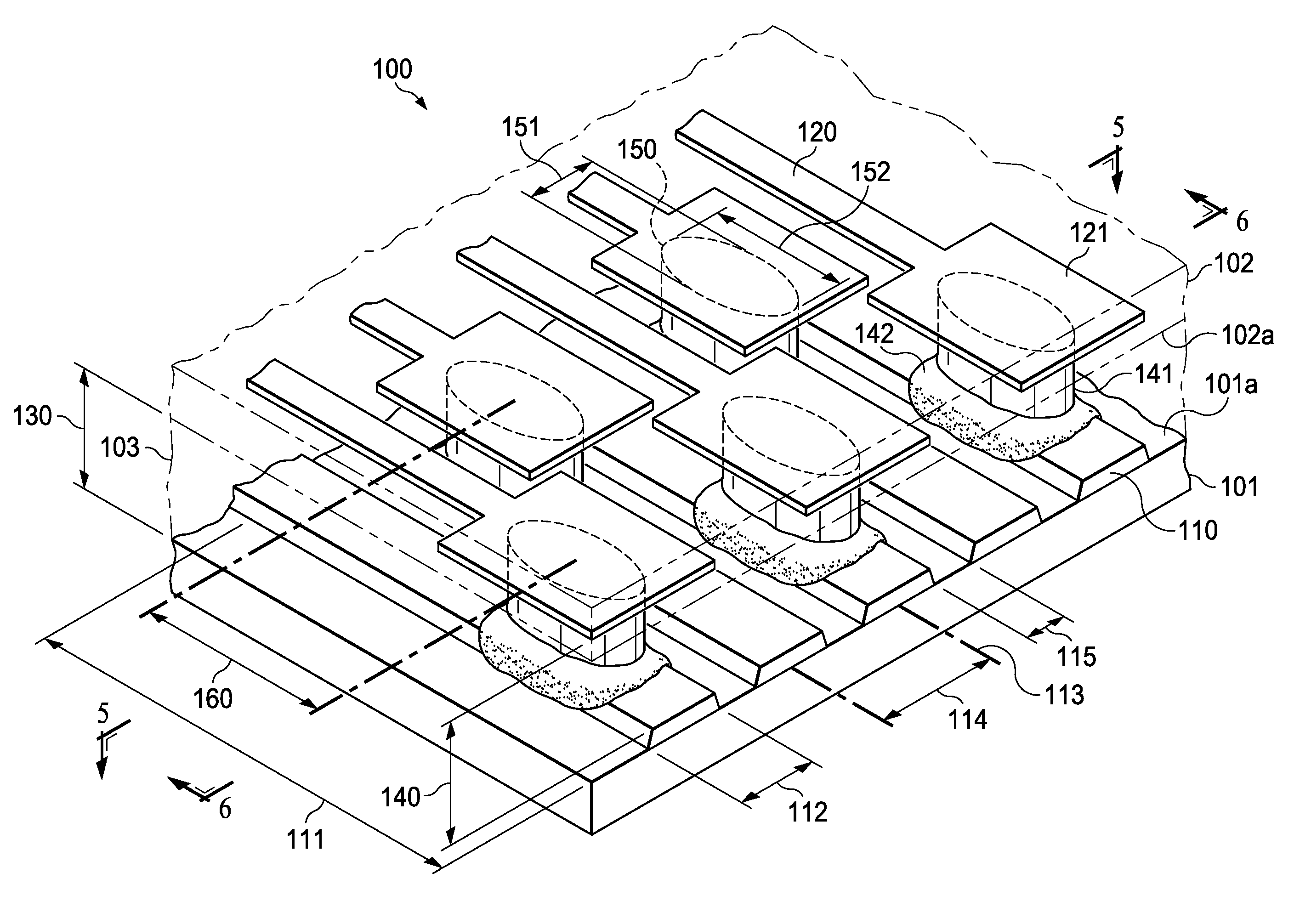
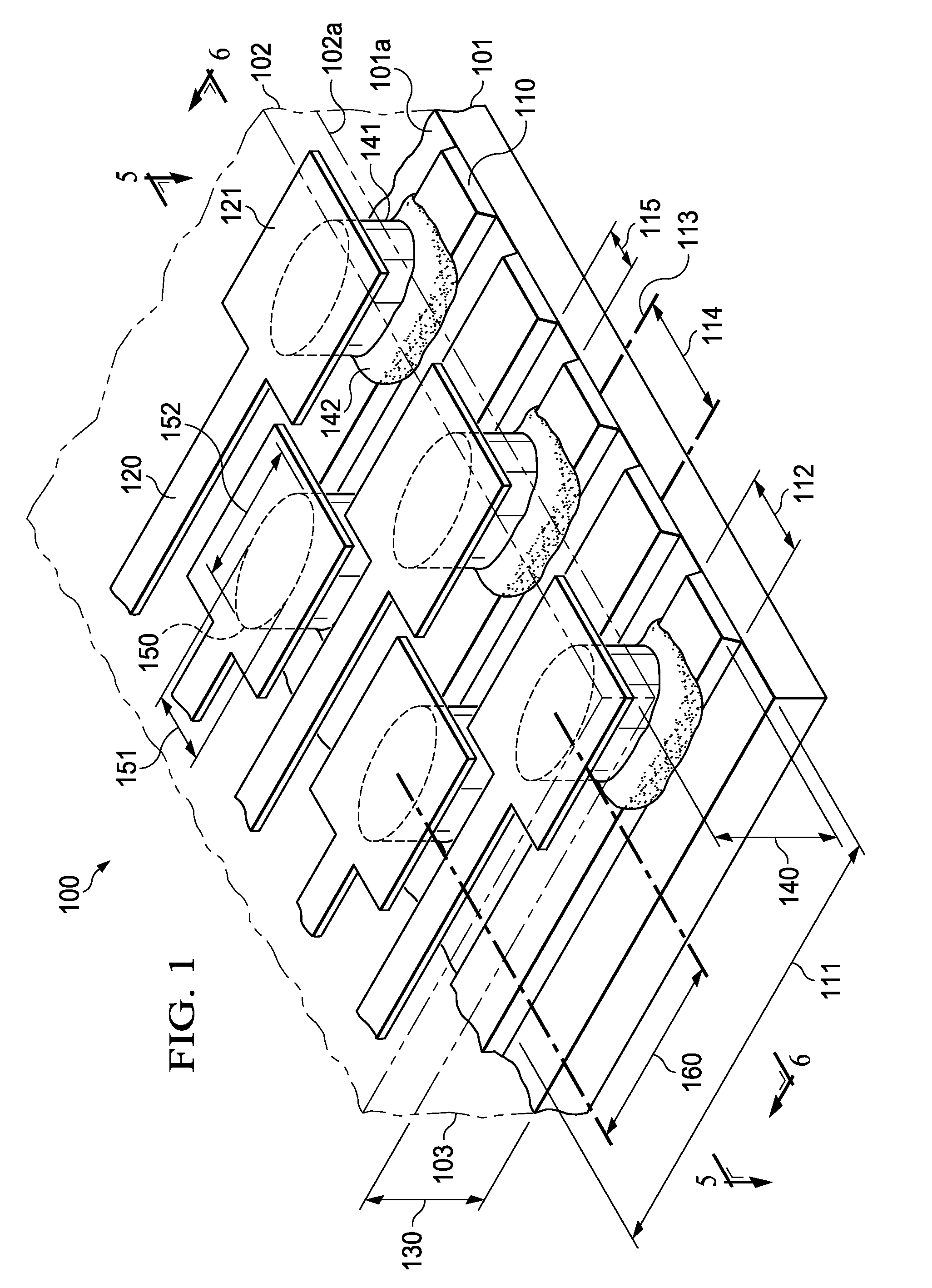
[0017]FIG. 1 illustrates an exemplary embodiment of the invention, generally designated 100, which includes a semiconductor chip 102 assembled by flip-chip methodology on an insulating substrate 101. The substrate has a first surface 101a and a plurality of conductive traces 110. These traces may be placed on the substrate surface, as shown in FIG. 1, or may be level with the substrate surface. As FIG. 1 indicates, traces 110 have a first length 111, which is sufficient to accommodate the attachment of the connections to the chip 102; in FIG. 1, the attachments are positioned in a staggered arrangement relative to each other. For the extent of first length 111, the traces 110 are straight and parallel to each other. Traces 110 have a first width 112, which is uniform along first length 111. For the straight length, each trace 110 has a centerline 113. The distance between two adjacent trace centerlines determines the trace pitch 114. For the plurality of traces 110 shown in FIG. 1, ...


PUM


Abstract

A semiconductor chip (102) assembled on a substrate (101). The substrate has a first surface (101a) including conductive traces (110), which have a first length (111) and a first width (112), the first width being uniform along the first length, and further a pitch (114) to respective adjacent traces. The semiconductor chip has a second surface (102a) including contact pads (121); the second surface faces the first surface spaced apart by a gap (130). A conductive pillar (140) contacts each contact pad; the pillar includes a metal core (141) and a solder body (142), which connects the core to the respective trace across the gap. The pillar core (141) has an oblong cross section of a second width (151) and a second length (152) greater than the second width. Trace pitch (141) is equal to or smaller than twice the second width (151). The trace pitch is equal to or smaller than the second length (152).

Description

FIELD OF THE INVENTION[0001]The present invention is related in general to the field of semiconductor devices and processes, and more specifically to the structure and fabrication method of semiconductor chips with oblong pillar-shaped bumps designed for fine pitch interconnect and high stress tolerance.DESCRIPTION OF RELATED ART[0002]Electronic applications such as handheld telephones and other wireless products offer the customer an ever increasing number of features, while the sizes of the telephones and other products keep shrinking. As a consequence, there is an ongoing trend for the semiconductor devices inside these products to miniaturize the size of the devices while increasing the number of functional device terminals. The shrinking device dimensions at increasing terminal numbers translate into ever finer pitch of the interconnections used by these devices. Today, the preferred technology for interconnecting a semiconductor chip to a substrate is by forming metallic bumps...

Claims


Application Information

Patent Timeline
Patent Type & Authority Applications(United States)
IPC IPC(8): H01L23/498
CPCH01L24/16H01L2224/0401H01L2924/01033H01L2924/00013H01L24/14H01L2224/13012H01L2224/13147H01L2924/01013H01L2924/01014H01L2924/01029H01L2924/01046H01L2924/01078H01L2924/01079H01L2924/01082H01L2924/014H01L2924/14H01L23/49811H01L24/06H01L24/13H01L2924/00014H01L2224/13099H01L2224/16238H01L2224/13013H01L2224/13014H01L2924/00012H01L2224/05147H01L2224/0558H01L2224/05638H01L2224/05655H01L2224/13005
Inventor CASTRO, ABRAM M.GERBER, MARK A.
Owner TEXAS INSTR INC
Why Eureka
Try Eureka