
Layered inductor

Inactive Publication Date: 2010-08-05
NGK INSULATORS LTD
View PDF4 Cites 27 Cited by
  • Summary
  • Abstract
  • Description
  • Claims
  • Application Information

AI Technical Summary

Benefits of technology

[0011]Meanwhile, a gel cast method (gel-casting method) is a method where a ceramic slurry in which ceramic powders and gelatinizing agents are dispersed in the dispersion media (solvent) is poured into a mold, and thereafter, the slurry is fixed / hardened according to an urethane reaction so as to obtain a formed-compact-before-fired (pre-sintered body, pre-fired body). According to the gel cast method, a formed compact having a desired shape to be formed by the mold can easily be obtained, because an amount of shrinkage of the slurry when the slurry is dried (or when the solvent vaporizes) is small compared with the general forming method.
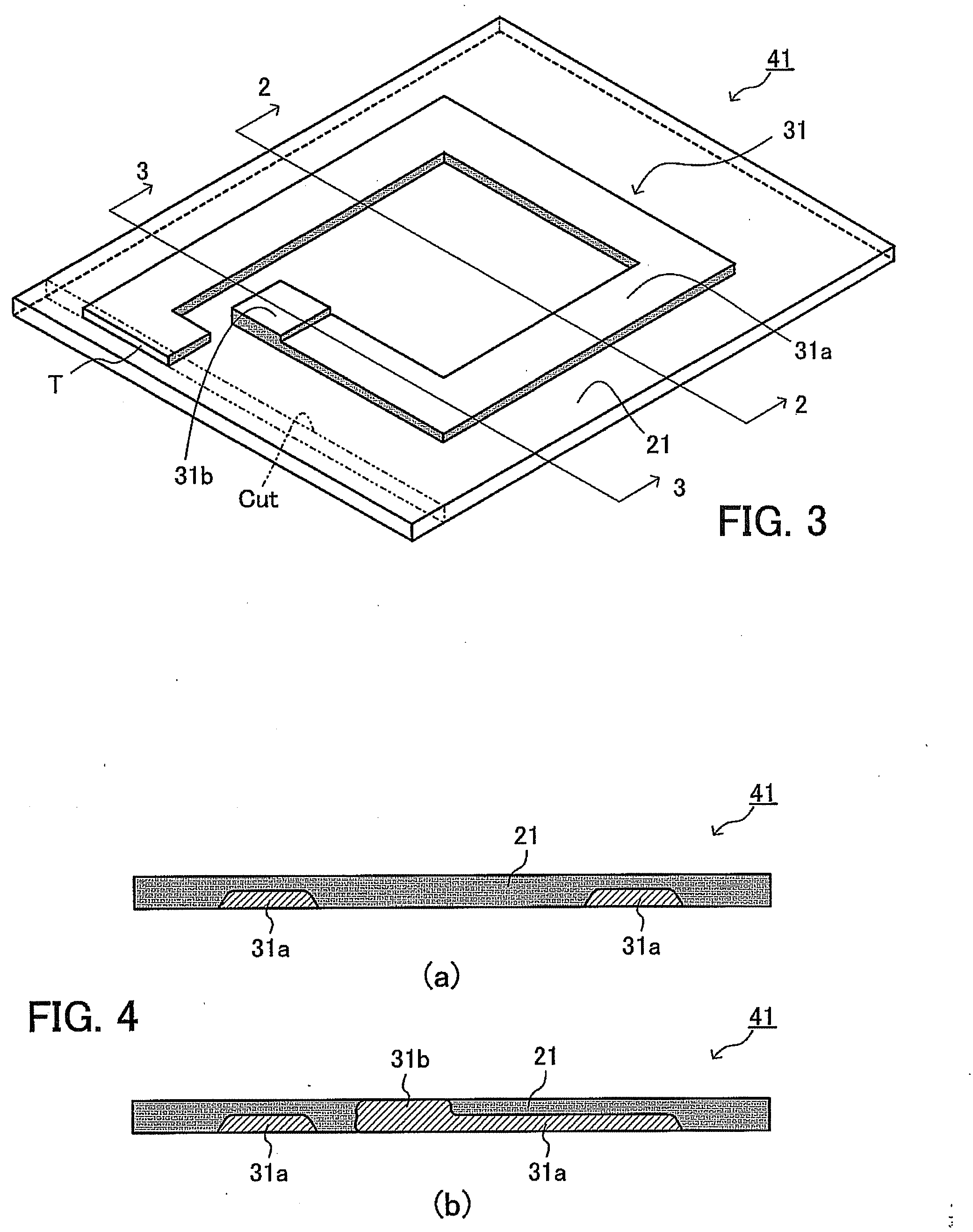
[0012]In view of the above, the applicant is trying to manufacture “a ceramic green sheet in which a conductive layer is buried into a magnetic layer (e.g., ferrite layer)” which has a uniform thickness, by using the gel cast method. Specifically, a conductive layer having a predetermined shape is firstly formed on an upper surface of a lower mold by a printing method. Subsequently, an upper mold is placed on the lower mold to form / provide a space having a constant height to hold / store / accommodate the conductive layer. Thereafter, “a ceramic slurry, in which ferrite powders as ceramic powders and gelatinizing agents are dispersed in dispersion media” is poured into the space to be fixed / hardened in order to form a ferrite-sheet-before-fired in which the conductive layer is buried. As a result, the sheet-before-fired, having the uniform thickness, in which the conductive layer has an increased thickness, can be manufactured / produced.
[0013]This sheet has the uniform thickness. Accordingly, in a layered body obtained by layering the sheets, “a thickness of a portion where the conductive layers are formed” and “a thickness of a portion where no conductive layer is formed” are equal to each other. This allows the thickness of the conductive layer to be increased without increasing a distance (a pitch) between conductive layers adjacent to each other in a direction of layering (in the other words, without decreasing the inductance), since the problem such as the delamination hardly occurs. As a result, it is possible to decrease the resistance of the layered inductor without decreasing the inductance of the layered inductor.

Problems solved by technology

In the compact / body formed according to the gel cast method, the ceramic powders are captured in polymer networks, and the amount of shrinkage during drying is therefore small, however, a density of the compact / body becomes small compared to the compact / body formed according to the printing-layering method, and the tape layering method, etc.
This causes a large difference in an amount of shrinkage between the conductive layers formed by the printing method and the magnetic layers formed by the gel cast method, while they are fired.
As a result, while firing, the structural defect, such as “gaps extending in a direction parallel to layers (hereinafter, referred to as “a side direction gap” or “a side direction crack”) may occur, or the desired electrical characteristics may not be obtained.
Particularly, if a ratio of a volume of the conductive layers to a volume of the inductor is made larger in order to reduce the resistance of the coil, the structural defect may occur prominently.
Accordingly, it turned out that there arises a problem that the inductance decreases extremely.

Method used


Image

  • Layered inductor
  • Layered inductor
  • Layered inductor

Examples


Embodiment Construction

[0072]Next will be described layered inductors (layered type inductors, multi-layered inductors) according to embodiments of the present invention with reference to the drawings.

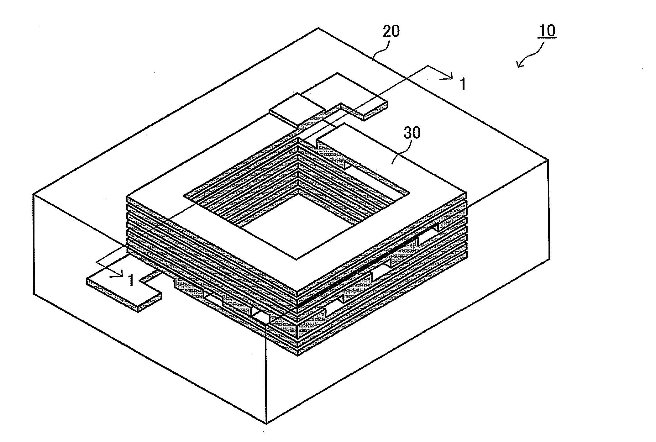
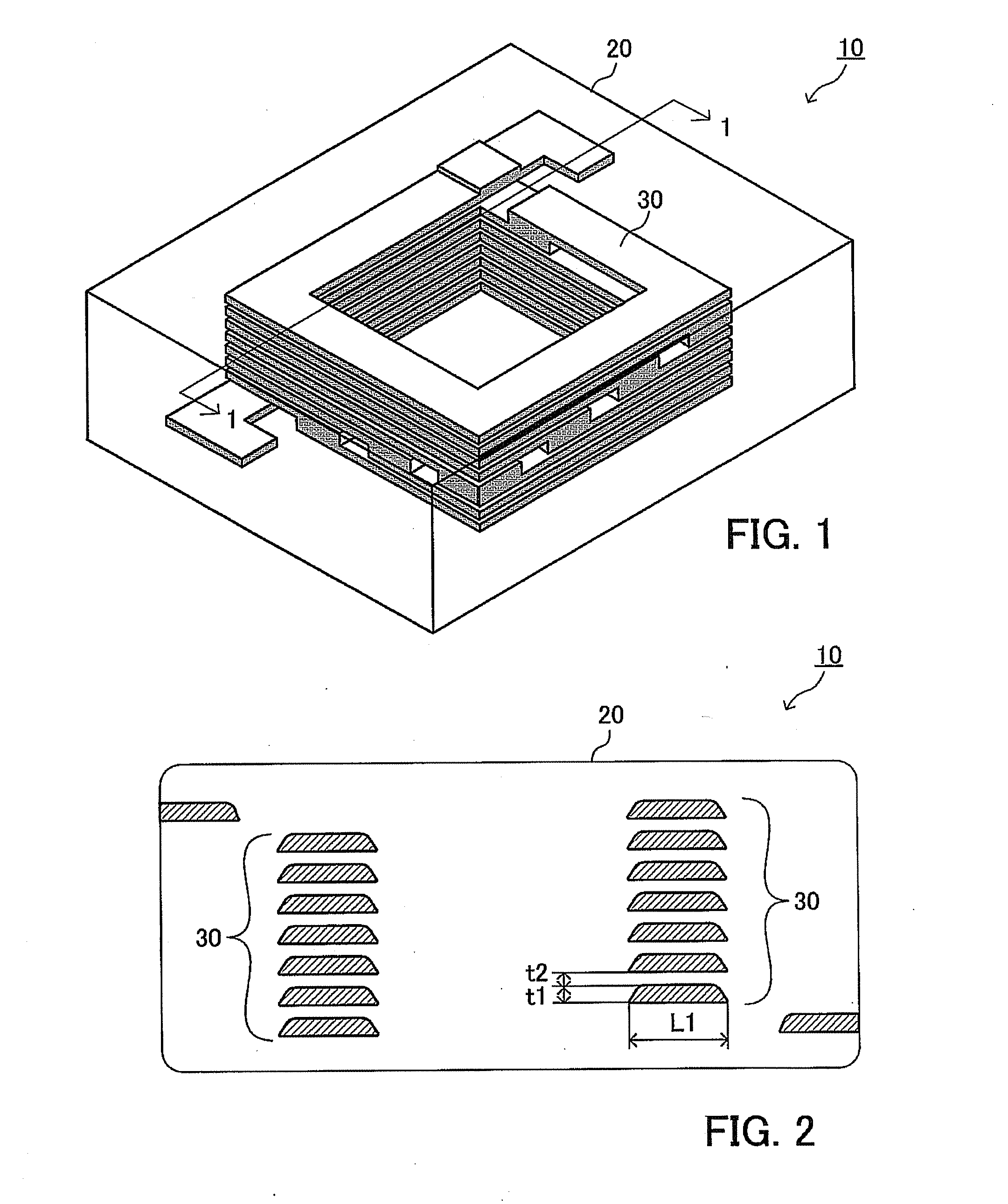
[0073]FIG. 1 is a perspective view of a layered inductor 10 according to an embodiment of the present invention. FIG. 2 is a vertical cross-sectional view of the layered inductor 10, wherein the inductor is cut by a plane along a line 1-1 of FIG. 1. A shape of the layered inductor 10 is a rectangular parallelepiped, having a depth, a width, and a height, each of which is about a few millimeters. The layered inductor 10 comprises a magnetic body portion 20 containing ferrite as a magnetic substance (i.e., ferrite-based magnetic body 20) and coil portion 30 containing silver (Ag) as a conductive material (i.e., silver-based coil portion 30). The magnetic body portion 20 comprises a plurality of magnetic layers integrated / united by being fired. The coil portion 30 comprises a plurality of conductive layers inte...


PUM


Abstract

A layered inductor 10 is manufactured by layering “silver-based conductive layers” and “ferrite-based magnetic layers” and simultaneously firing these layers. The conductive layers are via-connected to form a helical coil 30. A shape of a cross sectional surface of the conductive layer, cut by a plane perpendicular to a longitudinal direction of each of the conductive layers is a substantial trapezoid shape, having an upper base and a lower base. A base angle θ of the trapezoid shape at both ends of the lower base is equal to or greater than 50° and is smaller than or equal to 80°.

Description

FIELD OF THE INVENTION[0001]The present invention relates to a layered inductor in which silver-based conductive layers and ferrite-based magnetic layers are layered, and simultaneously fired / sintered.BACK GROUND OF THE INVENTION[0002]Conventionally, a compact power inductor (chip inductor) has been used for realizing functions such as suppressing noise, rectification, and smoothing signals, for example, in a power supply circuit for semiconductors, a power circuit for a DC-DC convertor, and so on. A large inductance and a low resistance are required for the compact power inductor.[0003]One of the compact power inductors is a layered inductor (multi-layered inductor). As shown in FIG. 36 showing a perspective view of the layered inductor 110, the layered inductor 110 typically comprises a magnetic body 111 and a coil 112 buried in the magnetic body 111.[0004]The coil 112 comprises conductive layers (conductive thin plates) 112A, each of which is formed so as to have a predetermined ...

Claims


Application Information

Patent Timeline
IPC IPC(8): H01F5/00
CPCH01F17/0013H01F2017/0066H01F2017/002H01F41/046H05K1/165H05K3/4629H05K2201/083H05K2201/09672H05K2201/098
Inventor OZAWA, SHUICHISHIMOGAWA, NATSUMITAKEUCHI, KATSUYUKIAISAKA, YUKIO
Owner NGK INSULATORS LTD
Learn More