Patterned wafer inspection system using a non-vibrating contact potential difference sensor

a contact potential difference and sensor technology, applied in semiconductor/solid-state device testing/measurement, image enhancement, instruments, etc., can solve the problems of inability to detect sub-monolayer chemical non-uniformities, inability to detect pre-existing charge variation across the wafer, and limited inspection technology available for patterned wafer inspection, etc., to achieve the effect of quick surface imaging and convenient data analysis

Inactive Publication Date: 2010-08-05
QCEPT INVESTMENTS LLC
View PDF4 Cites 6 Cited by
  • Summary
  • Abstract
  • Description
  • Claims
  • Application Information

AI Technical Summary

Benefits of technology

[0006]The system and methods described in this invention provide an enhanced application of a non-vibrating contact potential difference inspection system that allows the rapid imaging of surfaces and the detection of work function non-uniformities on surfaces that contain a repeating or other preprogrammed pattern of relative work function values. This capability is particularly useful for the detection of chemical or charge-related defects on patterned semiconductor wafers, or other preprogrammed pattern arrangements on wafers, during the manufacturing process.
[0007]In preferred embodiments the wafer and sensor are moved relative to each other to produce a contact potential difference signal cha

Problems solved by technology

The technologies available for the inspection of patterned wafers are very limited.
These types of systems are not however able to detect sub-monolayer chemical non-uniformities in, or on, the wafer surface; and are not able to detect pre-existing charge variation across the wafer.
Technologies that are capable of detecting small chemical variations are not suitable for the inspection of patterned wafers because they lack the speed or resolution to inspect the whole wafer, are destructive, or are not suitable for use on complex surfaces that include significant material and geometric variations.
For example, Time-of-Flight Secondary Ion Mass Spectrometry (TOF-SIMS) is often used to characterize the chemical

Method used


Image

  • Patterned wafer inspection system using a non-vibrating contact potential difference sensor
  • Patterned wafer inspection system using a non-vibrating contact potential difference sensor
  • Patterned wafer inspection system using a non-vibrating contact potential difference sensor

Examples


example i

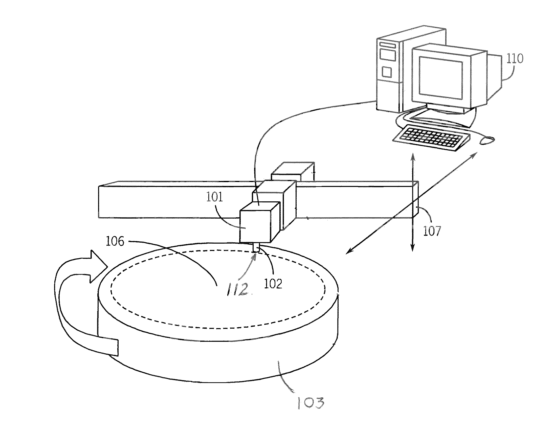
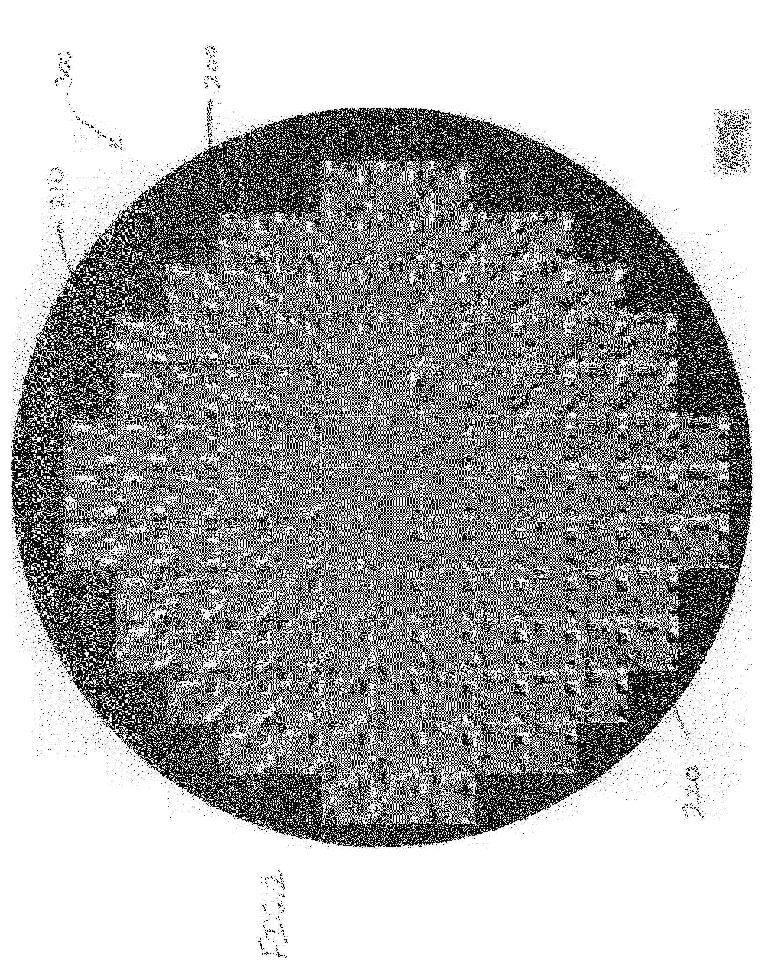
[0047]A standard silicon test wafer 106 with a pattern applied thereto was obtained from a commercial source which routinely produces semi-conductor grade starting wafers. This wafer consisted of a repeating test pattern die that was created using a chemical mechanical planarization process. The pattern consisted of copper and a dielectric material. Drops of chemical contaminant were then deposited along radii of the wafer using a jet printing process. This wafer 106 was inspected by the system 100 to provide the image 300 shown in FIG. 2. This image 300 resulted from radially scanning the patterned wafer 106 with a non-vibrating contact potential differential sensor 101. A graphic display showing the individual die 200 is overlaid on the image. Note that the appearance of dice changes depending on the location of the die 200 on the wafer surface. The polarity (light or dark) of the pattern edges changes depending on the direction of travel of the scanning probe tip and the signal m...

example ii

[0048]FIG. 3 shows a magnified image of a die 200 in the upper right corner of the image in FIG. 2 near the edge of the wafer 106; and the scanned image shows differential data, i.e. a signal generated at the edges of features.

example iii

[0049]FIG. 4 shows the same die 200 as FIG. 3 after an integration step and the integrated image shows regions of relative work function.


PUM


Abstract

A method and system for inspecting a surface of a material having a repeating pattern of relative work function. The method and system processes sensor data to identify data characteristic of the repeating pattern, and the sensor data is then further processed to remove the data characteristic of the repeating data, leading to a characteristic of non-uniformities of the material surface.

Description

CROSS-REFERENCE TO RELATED PATENT APPLICATIONS[0001]This application claims priority from U.S. Provisional Application No. 61 / 149,605, filed Feb. 3, 2009. The contents of this application is incorporated herein by reference in its entirety.FIELD OF THE INVENTION[0002]The present invention is directed to methods and systems for the inspection of surfaces and materials, including semiconductor surfaces and semiconductor materials. More particularly, the present invention is directed to methods for detecting and measuring surface or subsurface non-uniformities and / or charges using a non-vibrating contact potential difference sensor on a surface that contains a repeating pattern of work function variation.BACKGROUND OF THE INVENTION[0003]The function, reliability and performance of semiconductor devices depend on the use of semiconductor materials and surfaces which are clean and uniform. Billions of dollars and countless man-hours have been spent developing, characterizing, and optimiz...

Claims


Application Information

Patent Timeline
IPC IPC(8): G06F19/00
CPCG06T7/0006H01L22/14G06T2207/30148H01L22/00
Inventor SCHULZE, MARK A.LIU, JUNHAWTHOME, JEFFREY ALAN
Owner QCEPT INVESTMENTS LLC
Why Eureka
Try Eureka