Heat spreader for semiconductor device and method for manufacturing the same

a technology for semiconductor devices and heat spreaders, which is applied in the direction of manufacturing tools, semiconductor/solid-state device details, lighting and heating apparatus, etc., can solve the problems of heavy weight of copper-molybdenum alloy plates, problems such as a great challenge, and disadvantages, so as to avoid easy fracturing

Inactive Publication Date: 2010-08-19
ALLIED MATERIAL
View PDF2 Cites 35 Cited by
  • Summary
  • Abstract
  • Description
  • Claims
  • Application Information

AI Technical Summary

Benefits of technology

[0031]As described above, according to the present invention, obtained is a heat spreader for a semiconductor device in which a multitude of pin-shaped fins are joined so as to avoid easy frac

Problems solved by technology

However, the copper-molybdenum alloy plate has some drawbacks.
A first problem is that a weight thereof is heavy.
In particular, in a transport machine of which a reduction in a weight is required, this problem poses a great challenge.
A second problem is that it is suggested that a cooling efficiency cannot be increased because the heat-conductive grease 7 is interposed between the copper-molybdenum alloy plate 6 and the cooling unit 500 as shown in FIG. 6, though the second problem is not a drawback of the copper-molybdenum alloy plate itself.
In view of corrosion of aluminum, it is difficult to cause the radiator for an automobile engine to function as a radiator for the heat dissipation structure for a semiconductor device.
However, not only such a countermeasure incurs an increase in a weight thereof but also i

Method used


Image

  • Heat spreader for semiconductor device and method for manufacturing the same
  • Heat spreader for semiconductor device and method for manufacturing the same
  • Heat spreader for semiconductor device and method for manufacturing the same

Examples


example 1

[0095]A silicon carbide powder which is manufactured by Pacific Rundum Co., Ltd. and has a purity of 99.5% and a granularity of #320, an aluminum alloy powder which is manufactured by Toyo Aluminum K.K. and whose JIS alloy number is A1070, and an auxiliary agent were mixed, and the mixed powders whose volume contents of the silicon carbide particles were 20%, 40%, 60%, 80%, and 85%, were prepared as starting materials of the base material 11 of the heat spreader 1.

[0096]As starting materials of the surface layers 12 of the heat spreader 1, aluminum alloy plates whose JIS alloy number were A1050, and had plane dimensions of 120 mm×120 mm and thicknesses of 0.05 mm, 0.1 mm, 0.2 mm, 0.4 mm, 0.8 mm, and 1.2 mm were prepared.

[0097]Each of the mixed powders prepared as mentioned above was sandwiched by two aluminum alloy plates and each compact was formed by applying a load of 700 tons thereto with a press so as to have a size of 120 mm×120 mm×3.1 mm, whereby compacts were prepared.

[0098]...

example 2

[0112]An influence of a heat conductivity of the plate-like member in the heat spreader 1 was investigated.

[0113]Upon preparing a test sample No. 6 by employing the same method as in Example 1, instead of the aluminum alloy powder, manufactured by Toyo Aluminum K.K., whose JIS alloy number is A1070, a powder was prepared as a starting material of the base material 11 such that magnesium of 6% by mass was added to an aluminum alloy powder whose alloy number is A1050 and the obtained powder was subjected to atomizing processing. By using powders obtained by blending, with varied blending ratios, this aluminum alloy powder with the magnesium added thereto and the aluminum alloy powder whose alloy number was A1050, test samples having different heat conductivities of the plate-like members, each of which was included in the heat spreader 1, were prepared.

[0114]Since as the starting material of the base material 11, the aluminum alloy powder with the magnesium added thereto was used, a h...

example 3

[0118]An influence of a thickness of the plate-like member in the heat spreader 1 was investigated.

[0119]Upon preparing test samples by employing the same method as in Example 1, with reference to the properties of the test sample No. 5, amounts of the mixed powder of the silicon carbide particles and the aluminum alloy powder, as the starting material of the base material 11, were adjusted, a thickness of each of the surface layers 12 of each thereof was set to be 0.1 mm and thicknesses of the whole plate-like member were set to be 0.4 mm, 0.5 mm, 1.0 mm, 2.0 mm, 4.0 mm, 6.0 mm, and 8.0 mm, whereby the plate-like members, each of which was included in the heat spreader 1, were prepared so as to have different thicknesses. Evaluation was conducted in the same manner as in Example 1.

[0120]The results are shown in Table 3.

TABLE 3Material CompositionPropertiesSurfaceLinearSiCLayerPlateAreaHeatExpansionIGBT Endurance TestPercentageThicknessThicknessProportionConductivityCoefficientLowMi...


PUM

PropertyMeasurementUnit
Lengthaaaaaaaaaa
Lengthaaaaaaaaaa
Lengthaaaaaaaaaa

Abstract

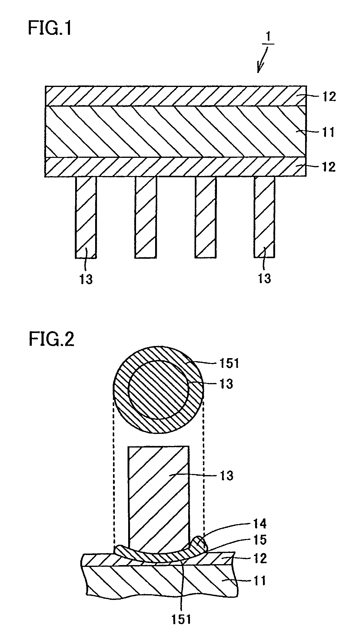
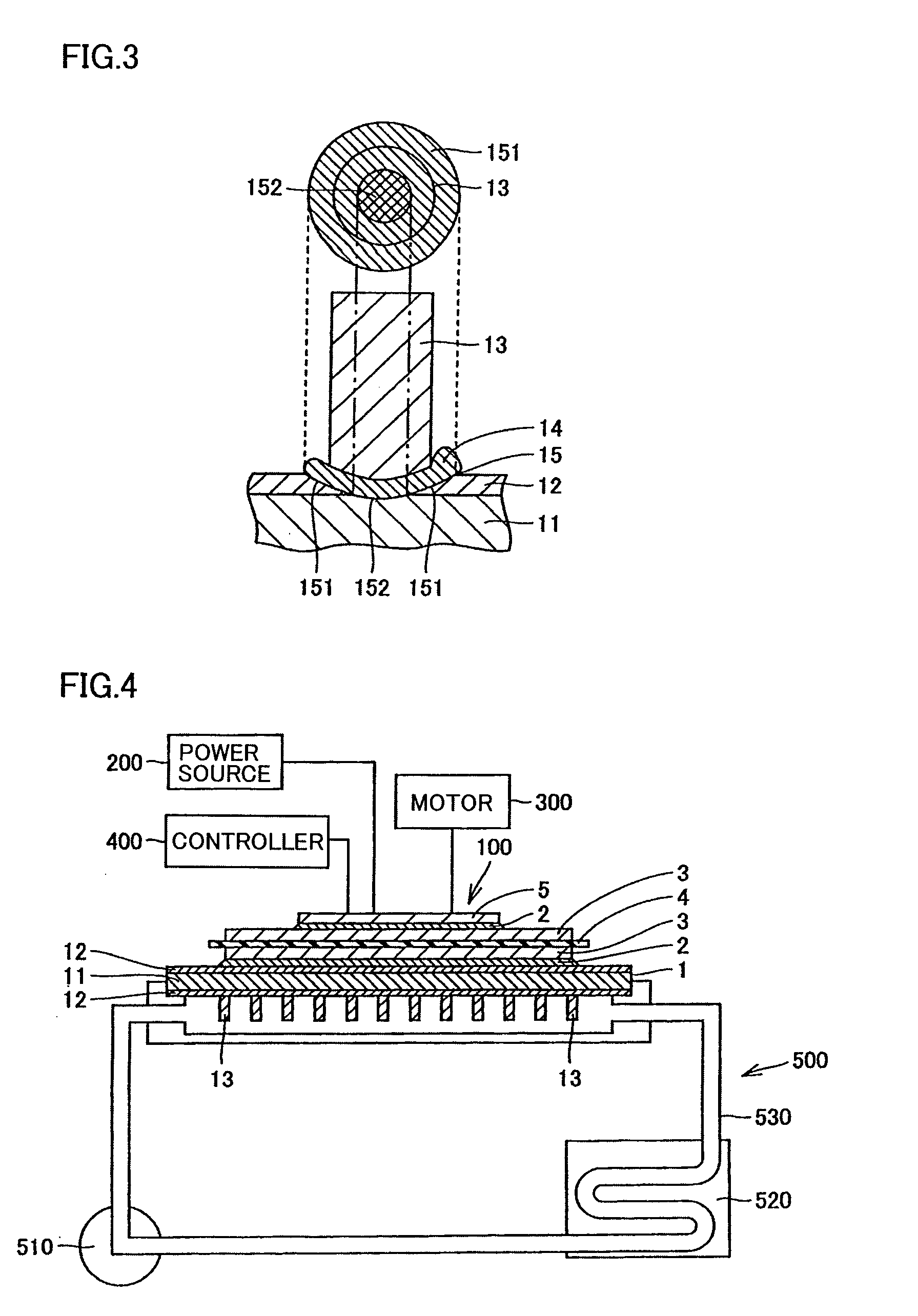
Provided are a heat spreader for a semiconductor device, which can be joined such that a multitude of pin-shaped fins are not easily fractured even when the heat spreader for a semiconductor device is incorporated in a heat dissipation structure for a semiconductor device, in which direct cooling is performed by using water, and a method for manufacturing the heat spreader for a semiconductor device. The heat spreader (1) for a semiconductor device comprises: a plurality of columnar members (13) joined onto at least one of surfaces of a plate-like member (11, 12) by stud welding; and a joining layer (14) formed between the plate-like member (11, 12) and the columnar members (13). The plate-like member (11, 12) includes a base material (11) and surface layers (12). The surface layers (12) and the columnar members (13) are made of a material containing aluminum or an aluminum alloy. A thickness of the plate-like member (11, 12) is 0.5 mm through 6 mm and a thickness of each of the surface layers (12) is 0.1 mm through 1 mm. The joining layer (14) has a joining interface (15) on a boundary with the plate-like member (11, 12). A proportion of an area of the joining interface (15) being present in the surface layer (12) is greater than or equal to 50% and less than or equal to 100%, converted in terms of a plane projected to the one of the surfaces of the plate-like member.

Description

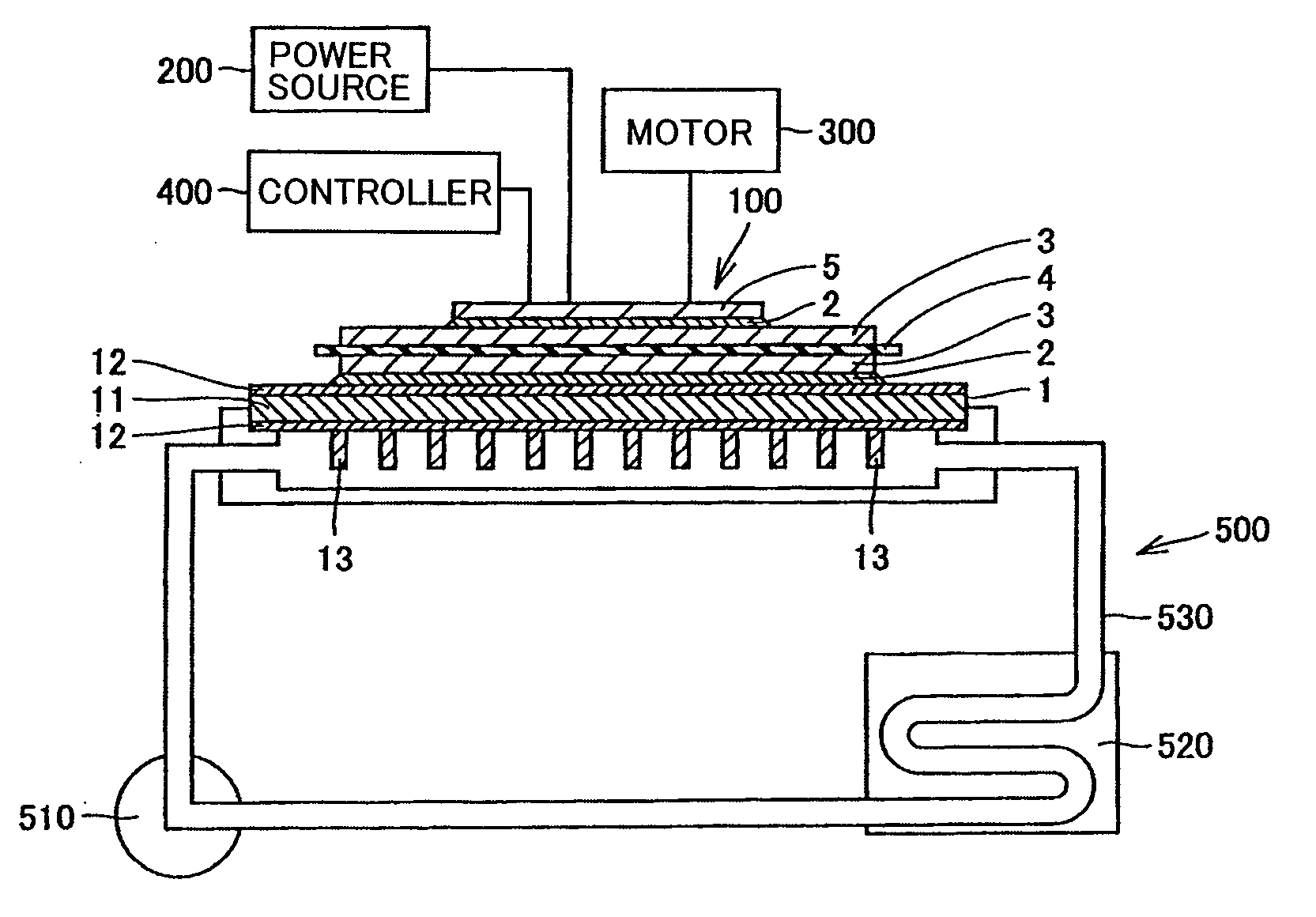
TECHNICAL FIELD[0001]The present invention relates generally to a heat spreader for a semiconductor device and a method for manufacturing the heat spreader for a semiconductor device, and, more particularly, to a heat spreader for a power device such as an insulated gate bipolar transistor (IGBT) which is mounted in an automobile or the like, and to a method for manufacturing the head spreader.BACKGROUND ART[0002]In a power device, such as an IGBT, used for controlling a motor in an electric train, an electric automobile, or the like, a heat spreader is used in order to effectively dissipate heat generated by a semiconductor device.[0003]FIG. 6 is a schematic diagram illustrating a heat dissipation structure for a semiconductor device, in which a conventional heat spreader is used.[0004]As shown in FIG. 6, aluminum layers 3 (or copper layers) are formed on both side surfaces of an insulating substrate 4 made of aluminum nitride, silicon nitride, alumina, or the like. On one surface ...

Claims


Application Information

Patent Timeline
IPC IPC(8): F28F7/00B23P15/26
CPCH01L23/3677H01L23/3735H01L23/473H01L2924/3011H01L2224/32225H01L2924/13055Y10T29/49393H01L2924/1305H01L2924/00
Inventor IKEDA, TOSHIYAKOYAMA, SHIGEKINISHIDA, SHINYA
Owner ALLIED MATERIAL
Why Eureka
Try Eureka