
Micro-Electro-Mechanical System Having Movable Element Integrated into Substrate-Based Package

Active Publication Date: 2010-08-19
TEXAS INSTR INC
View PDF20 Cites 69 Cited by
  • Summary
  • Abstract
  • Description
  • Claims
  • Application Information

AI Technical Summary

Benefits of technology

[0012]Applicants further discovered that the separation of movable and electronics parts provides greater system level integration with other components such as package-on-package MEMS, thus increasing the electrical product efficiency.
[0015]Exemplary MEMS of the pressure sensor family, operating on capacitive changes caused by a movable membrane, may offer 80% lower fabrication cost, when the membrane is integrated into the plastic device package instead of being fabricated in conventional manner as a portion of the silicon chip.

Problems solved by technology

Applicants saw that MEMS built on the surface or within the wafer by standard wafer fab technology and standard wafer fab lithographic methods is not only a high cost approach, but also limits the choice of materials and configuration available to the MEMS component, which have to be compatible with the standard wafer process.

Method used


Image

  • Micro-Electro-Mechanical System Having Movable Element Integrated into Substrate-Based Package
  • Micro-Electro-Mechanical System Having Movable Element Integrated into Substrate-Based Package
  • Micro-Electro-Mechanical System Having Movable Element Integrated into Substrate-Based Package

Examples


Embodiment Construction

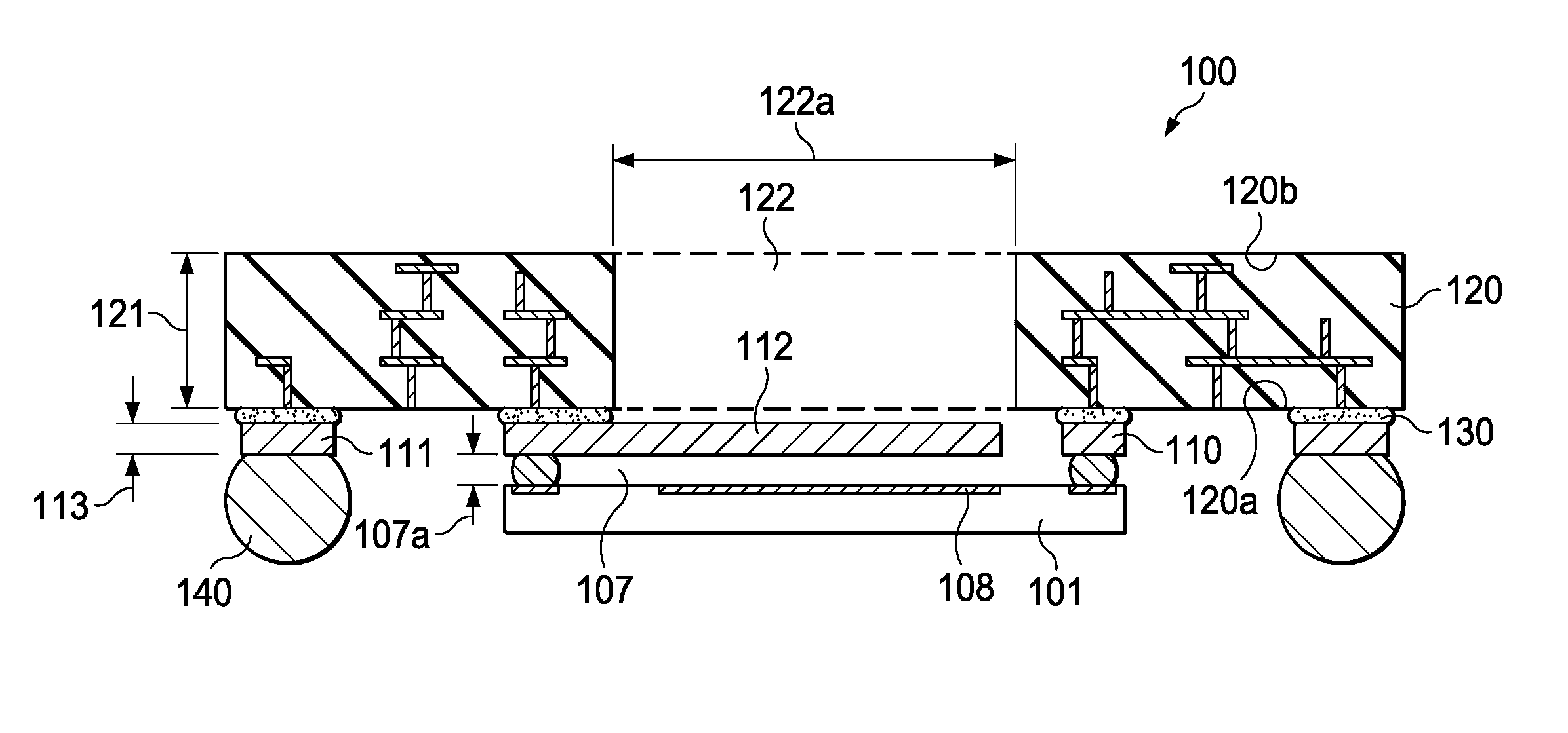
[0041]FIG. 1 illustrates a schematic cross section of an exemplary embodiment of the invention showing a micro-electro-mechanical system (MEMS) of the inertial sensor family, which operates as a capacitive accelerometer with displacement-dependent output signals. In these sensors, acceleration is transformed into the displacement of a movable mass or plate; the position change is measured as a change of the capacitance relative to a fixed plate. Capacitive accelerometers exhibit high sensitivity, good DC response and noise performance, low drift, and low power dissipation and temperature sensitivity. The exemplary MEMS, generally designated 100 in FIG. 1, is a system structured like QFN (Quad Flat No-lead) and SON (Small Outline No-Lead) type semiconductor devices.

[0042]In the embodiment of FIG. 1, an integrated circuit device, represented by chip 101, is flip-assembled on metallic pads 110. Flip-assembly typically utilizes conductive spacers such as solder balls or solder bodies to...


PUM

PropertyMeasurementUnit
Thicknessaaaaaaaaaa
Dielectric polarization enthalpyaaaaaaaaaa
Massaaaaaaaaaa

Abstract

Semiconductor-centered MEMS (100) integrates the movable MEMS parts, such as mechanical elements, flexible membranes, and sensors, with the low-cost device package, and leaving only the electronics and signal-processing parts in the integrated circuitry of the semiconductor chip. The package is substrate-based and has an opening through the thickness of the substrate. Substrate materials include polymer tapes with attached metal foil, and polymer-based and ceramic-based multi-metal-layer dielectric composites with attached metal foil. The movable part is formed from the metal foil attached to a substrate surface and extends at least partially across the opening. The chip is flip-assembled to span at least partially across the membrane, and is separated from the membrane by a gap.

Description

FIELD OF THE INVENTION[0001]The present invention is related in general to the field of semiconductor devices and processes, and more specifically to the structure and fabrication method of Micro-Electro-Mechanical systems (MEMS) having the movable element integrated into a substrate-based ball grid array package and the sensing element built on the integrated circuit.DESCRIPTION OF RELATED ART[0002]The wide variety of products collectively called Micro-Electro-Mechanical systems (MEMS) are small, low weight devices on the micrometer to millimeter scale produced on the basis of batch fabrication techniques similar to those used for semiconductor microelectronics devices. MEMS integrate mechanical elements, sensors, actuators, and electronics on a common carrier. MEMS have been developed to sense mechanical, thermal, chemical, radiant, magnetic, and biological quantities and inputs, and produce signals as outputs.[0003]MEMS may have parts moving mechanically under the influence of an...

Claims


Application Information

Patent Timeline
IPC IPC(8): H01L29/84H01L21/02
CPCB81C1/0023Y10T29/49117H01L25/50H01L2224/16225H01L2924/09701H01L2924/01066H01L2924/01087H01L2924/01322H01L29/84H01L2924/10253H01L25/165H01L2924/1461H01L2924/00H01L2224/0557H01L2224/05573H01L2224/05568H01L2924/00014H01L2224/05571H01L2224/0554H01L2224/05599H01L2224/0555H01L2224/0556
Inventor ZUNIGA-ORTIZ, EDGAR ROLANDOKRENIK, WILLIAM R.
Owner TEXAS INSTR INC
Features
  • Generate Ideas
  • Intellectual Property
  • Life Sciences
  • Materials
  • Tech Scout
  • Unparalleled Data Quality
  • Higher Quality Content
  • 60% Fewer Hallucinations
Learn More