
Vertical organic transistor, method for manufacturing the vertical organic transistor, and light emitting element

Active Publication Date: 2010-08-26
DAI NIPPON PRINTING CO LTD
View PDF8 Cites 19 Cited by
  • Summary
  • Abstract
  • Description
  • Claims
  • Application Information

AI Technical Summary

Benefits of technology

[0009]The present invention has been made with a view to solving the above problems of the prior art, and an object of the present invention is to provide a vertical organic transistor that can realize large current modulation and lowered production cost, and a method for manufacturing the vertical organic transistor. Another object of the present invention is to provide a light emitting element comprising the vertical organic transistor.

Problems solved by technology

Organic semiconductors used in organic field effect transistors, however, have low carrier mobility and thus suffer from problems such as small current modulation and low response speed.
Therefore, the area influenced by the voltage applied between the emitter electrode and the intermediate electrode is disadvantageously limited to a part around the edge of the striped intermediate electrodes.
Accordingly, the cost incurred in the manufacture of the vertical organic transistor is increased, and, thus, the technique disclosed in non-patent document 2 is not practical.
The problem leads to the loss of the advantage of the vertical organic transistor that the channel length can be reduced by a simple manufacturing method.

Method used


Image

  • Vertical organic transistor, method for manufacturing the vertical organic transistor, and light emitting element
  • Vertical organic transistor, method for manufacturing the vertical organic transistor, and light emitting element
  • Vertical organic transistor, method for manufacturing the vertical organic transistor, and light emitting element

Examples


experiment example 1

[0147]A 1 mm-thick glass substrate with a 150 nm-thick transparent ITO electrode (collector electrode) formed thereon was provided. The glass substrate with the ITO electrode was set in a vacuum chamber. A perylene-based pigment (Me-FTC) was formed to a thickness of 200 nm by vapor deposition on the ITO electrode to form a lower organic semiconductor layer. A 20 nm-thick aluminum metal film was then formed by vacuum vapor deposition on the lower organic semiconductor layer. In this case, the vapor deposition rate was set in the range of 0.1 nm / sec to 1 nm / sec so that the metal film is formed of a number of metallic particles (grains) having an average diameter of 30 nm. The film was actually formed at a vapor deposition rate of 1 nm / sec. The element with the aluminum metal film formed thereon (see FIG. 6 (A)) was held in an environment heated at 120° C. under the atmospheric environment to oxidize the periphery of the metallic particles constituting the aluminum metal film and thus ...

experiment example 2

[0149]A vertical organic transistor of Experiment Example 2 was manufactured in the same manner as in Experiment Example 1, except that the element with the aluminum metal film formed thereon was held at 25° C. under the atmospheric environment without heating.

experiment example 3

[0150]A vertical organic transistor of Experiment Example 3 was manufactured in the same manner as in Experiment Example 1, except that the element with the aluminum metal film formed thereon was held under a nitrogen gas atmosphere heated at 120° C.


PUM


Abstract

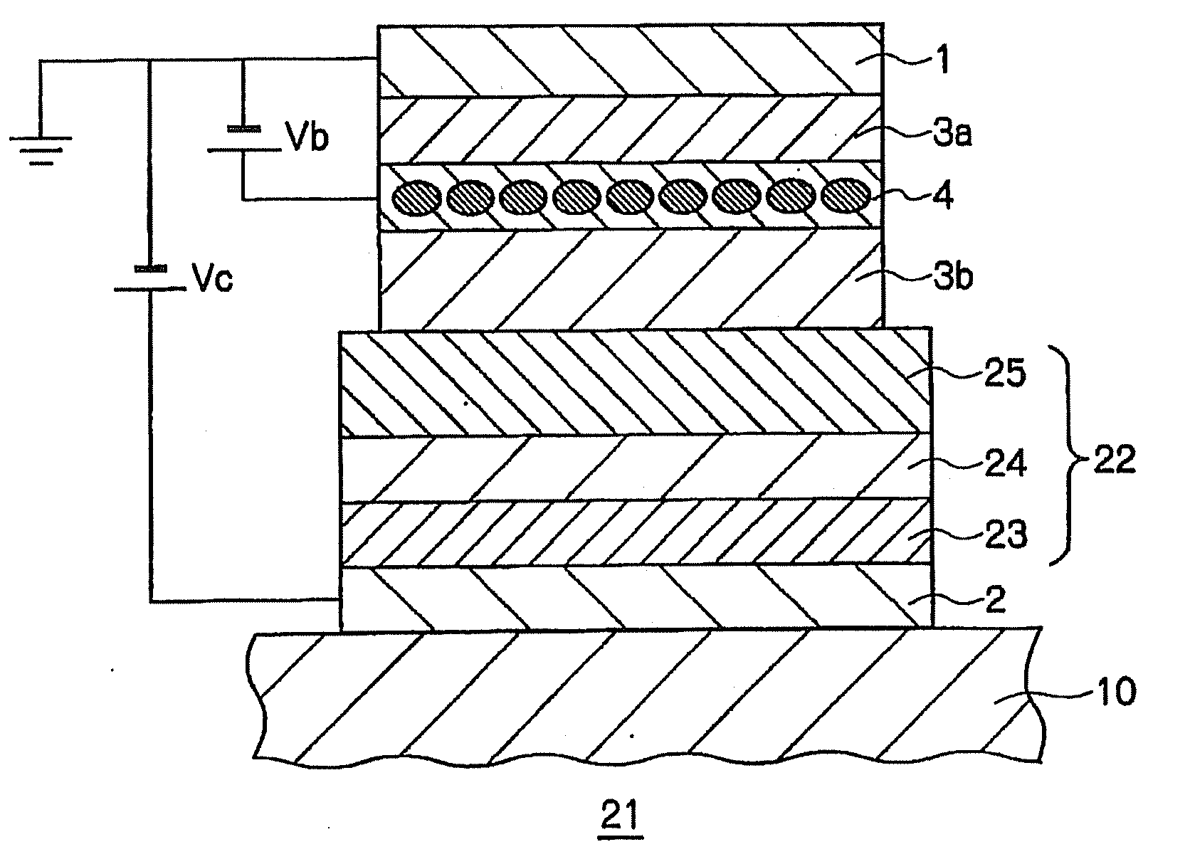
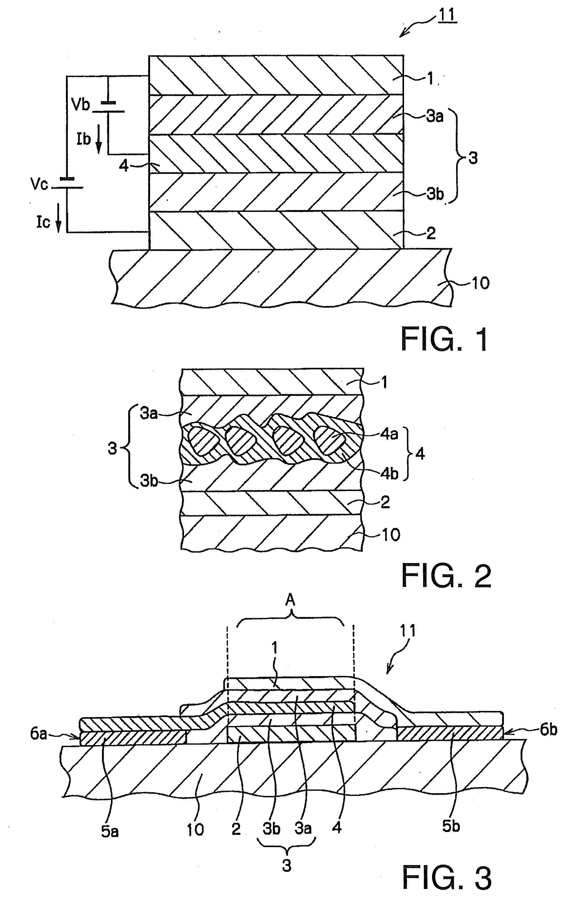
This invention provides a vertical organic transistor that can realize large current modulation and a reduction in production cost, and a method for manufacturing the vertical organic transistor. The vertical organic transistor comprises an upper electrode, a lower electrode, an organic semiconductor provided between both the electrodes, and an intermediate electrode provided within the organic semiconductor, the intermediate electrode being a layered continuous body comprising a continuous insulating metal compound and particulate metals distributed within the insulating metal compound.

Description

CROSS-REFERENCE TO RELATED APPLICATIONS[0001]This application is based upon and claims the benefit of priority under Article 4 of the Paris Convention from the prior Japanese Patent Applications No. 226664 / 2007, filed on Aug. 31, 2007 and No. 215068 / 2008, filed on Aug. 25, 2008, the entire contents of the specifications of which are incorporated herein by reference.FIELD OF INVENTION[0002]The present invention relates to a vertical organic transistor, a method for manufacturing the vertical organic transistor, and a light emitting element. More particularly, the present invention relates to a vertical organic transistor that can realize large current modulation and lowered production cost, a method for manufacturing the vertical organic transistor, and a light emitting element comprising a vertical organic transistor.BACKGROUND ART[0003]Organic field effect transistors (OFETs) have features such as low cost and good flexibility because organic transistors can be manufactured by a co...

Claims


Application Information

Patent Timeline
IPC IPC(8): H01L51/10H01L51/40
CPCB82Y20/00B82Y30/00H01L2251/5369H01L51/5296H01L51/057H10K10/491H10K50/30H10K2102/331H01L29/66H05B33/10H05B33/26H10K10/00H10K50/00
Inventor FUJIMOTO, SHINYAMAEDA, HIROKITSURUOKA, YOSHIAKI
Owner DAI NIPPON PRINTING CO LTD
Learn More