Supercharge Your Innovation With Domain-Expert AI Agents!

Light Emitting Apparatus

a technology of light-emitting apparatus and silicon, which is applied in the direction of electrical apparatus, semiconductor lasers, semiconductor devices, etc., can solve the problems of delayed signals, reduced speed, and the inability to grow high-quality iii-v structures directly on silicon (si)

Inactive Publication Date: 2010-08-26
PENN STATE RES FOUND
View PDF38 Cites 26 Cited by
  • Summary
  • Abstract
  • Description
  • Claims
  • Application Information

AI Technical Summary

Benefits of technology

[0021]Preferably, embodiments of the light emitting apparatus are sized and configured for manufacturing that utilizes one or more CMOS fabrication processes.

Problems solved by technology

Although the processing speed of the mentioned components can be elevated, the electrical resistance and capacitance of the wires connecting each integrated circuit chip and connecting the integrated circuit chips with the major components are increased due to the miniaturization, which can result in delayed signals and reduced speed.
While III-V laser junctions have been bonded to silicon waveguides where the emitted light is transmitted, the needed high-quality III-V structures typically cannot be grown directly on the silicon (Si).
Momentum conservation requires the presence of phonons to assist the radiative electron-hole recombination via the indirect band gap, which significantly lowers the radiative efficiency of germanium.
The density of the injected currents for the occurrence of radiative recombination and the onset of population inversion in the direct gap (Γ valley) is impractically high in bulk for Ge or SiGe based media.
In addition, carrier trapping and de-trapping cycles in the insulator often accompany the electron tunneling process, which further reduce the efficiency of the device.

Method used


Image

  • Light Emitting Apparatus
  • Light Emitting Apparatus
  • Light Emitting Apparatus

Examples


Embodiment Construction

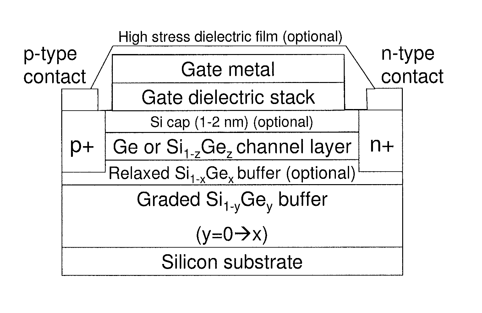
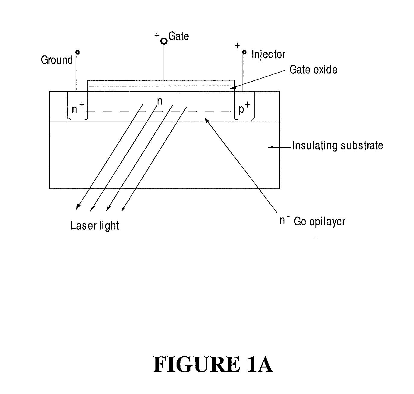
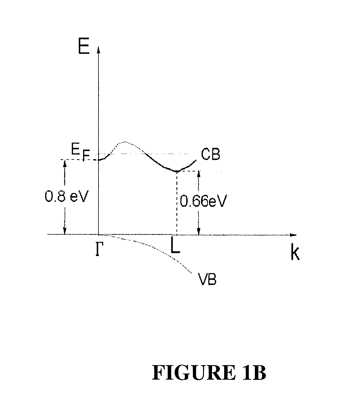
[0032]A germanium gain medium in an efficient light source preferably (1) exhibits direct band transition to eliminate the dependence on the phonon density in the material, (2) exhibits high radiation efficiency even at low or intermediate injection levels, (3) features low impurity doping concentration for reduced density of nonradiative recombination centers and low Auger recombination rate, and (4) avoids tunnel injection of carriers where carrier injection efficiency is lowered by carrier trapping and de-trapping cycles. None of the existing technologies can satisfy all of the above requirements simultaneously. Instead, conventional techniques try and provide a design that meets or optimizes only some of the above identified preferences.

[0033]It is contemplated that direct band radiation from germanium and silicon-germanium based on free electron accumulation / inversion in metal-oxide (insulator)-semiconductor (MOS / MIS) and modulation-doped (MOD) heterojunctions can provide a lig...


PUM


Abstract

A light emitting apparatus may include a gate metal positioned between a p-type contact and an n-type contact, a gate oxide or other dielectric stack positioned below and attached to the gate metal, a Ge or Si1-zGez channel positioned below and attached to the gate dielectric stack, a buffer, and a silicon substrate positioned below and attached to the buffer. The light emitting apparatus may alternatively include a gate metal positioned between a p-type contact and an n-type contact, a wide bandgap semiconductor positioned below and attached to the gate metal, a Ge or Si1-zGez channel positioned below and attached to the wide bandgap semiconductor, a buffer, and a silicon substrate positioned below and attached to the buffer. Embodiments of the light emitting apparatus may be configured for use in current-injected on-chip lasers, light emitting diodes or other light emitting devices.

Description

CROSS REFERENCE TO RELATED APPLICATION[0001]The present application claims priority to U.S. Provisional Patent Application No. 61 / 154,601, filed on Feb. 23, 2009. The entirety of U.S. Provisional Patent Application No. 61 / 154,601 is incorporated by reference herein.FIELD OF THE INVENTION[0002]The present invention relates to light emitting apparatuses such as semiconductors, light emitting diodes (LEDs), laser diodes and other light emitting devices.BACKGROUND OF THE INVENTION[0003]Basic components of a computer and other electronic devices include memory, central processing units, a power source and various circuits. Integrated circuit chips are often utilized in such devices. Although the processing speed of the mentioned components can be elevated, the electrical resistance and capacitance of the wires connecting each integrated circuit chip and connecting the integrated circuit chips with the major components are increased due to the miniaturization, which can result in delayed ...

Claims


Application Information

Patent Timeline
Patent Type & Authority Applications(United States)
IPC IPC(8): H01L33/00
CPCH01L33/0041H01S5/3031H01S5/3009H01L33/34Y10S438/933
Inventor XU, JIANASHOK, S.
Owner PENN STATE RES FOUND
Features
  • R&D
  • Intellectual Property
  • Life Sciences
  • Materials
  • Tech Scout
  • Unparalleled Data Quality
  • Higher Quality Content
  • 60% Fewer Hallucinations
Learn More